Smoothieboard V2 Prime Schematic Reference
This page provides a complete technical reference for the Smoothieboard V2 Prime hardware, extracted from the KiCad schematics. It covers all major subsystems including the microcontroller, power system, motor drivers, MOSFETs, inputs, and expansion headers.
smoothiev2-prime-2660.pdf (KiCad 5.1.9)Board Type: TMC2660 variant (Board ID 1)
Schematic Pages: 13 sheets
Schematic Page Overview
Click on any schematic image to view full size.
Main Sheet (Page 1)
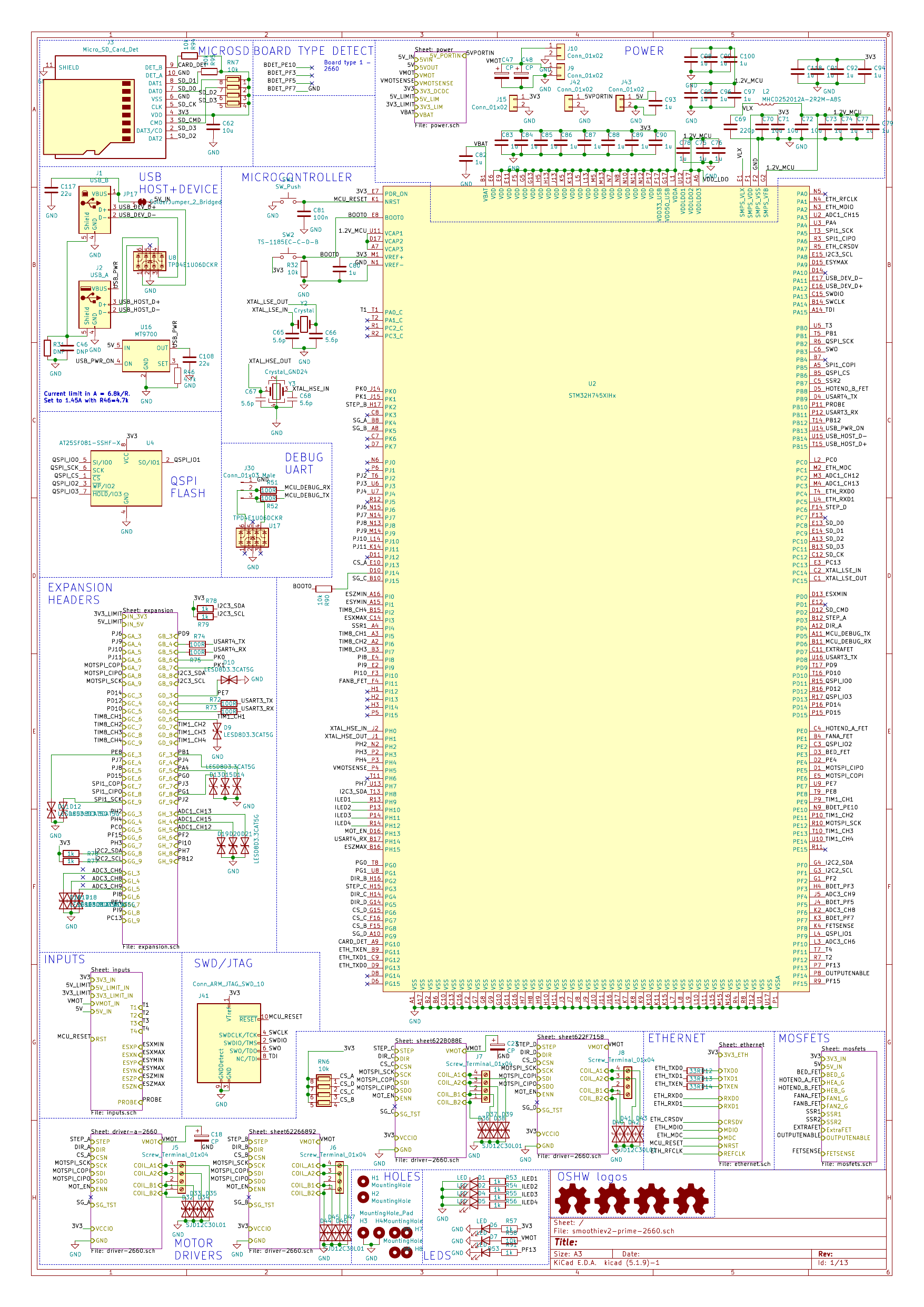
The main sheet contains the STM32H745 microcontroller and top-level connections to all hierarchical blocks.
Ethernet (Page 2)
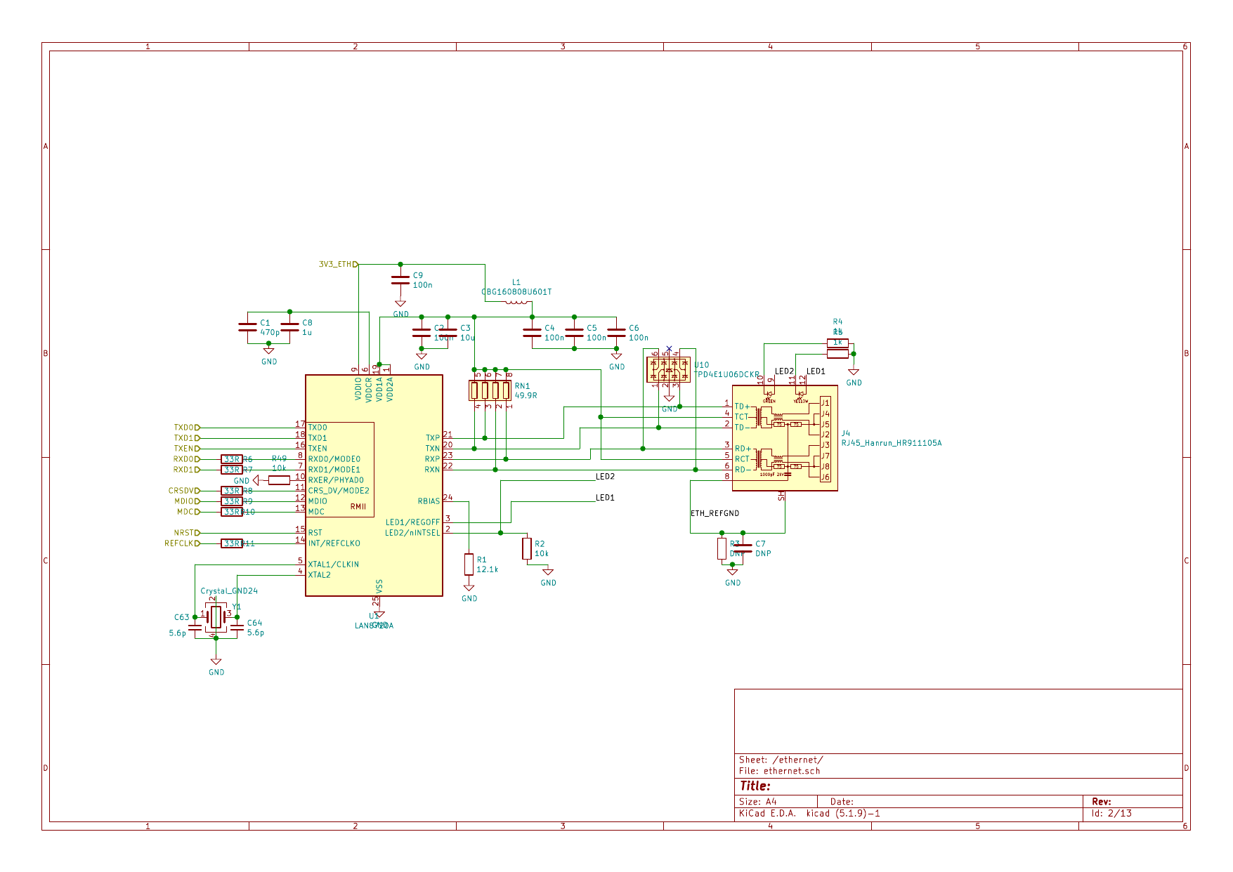
Ethernet PHY and RJ45 connector with auto-MDIX support.
MOSFETs (Page 3)
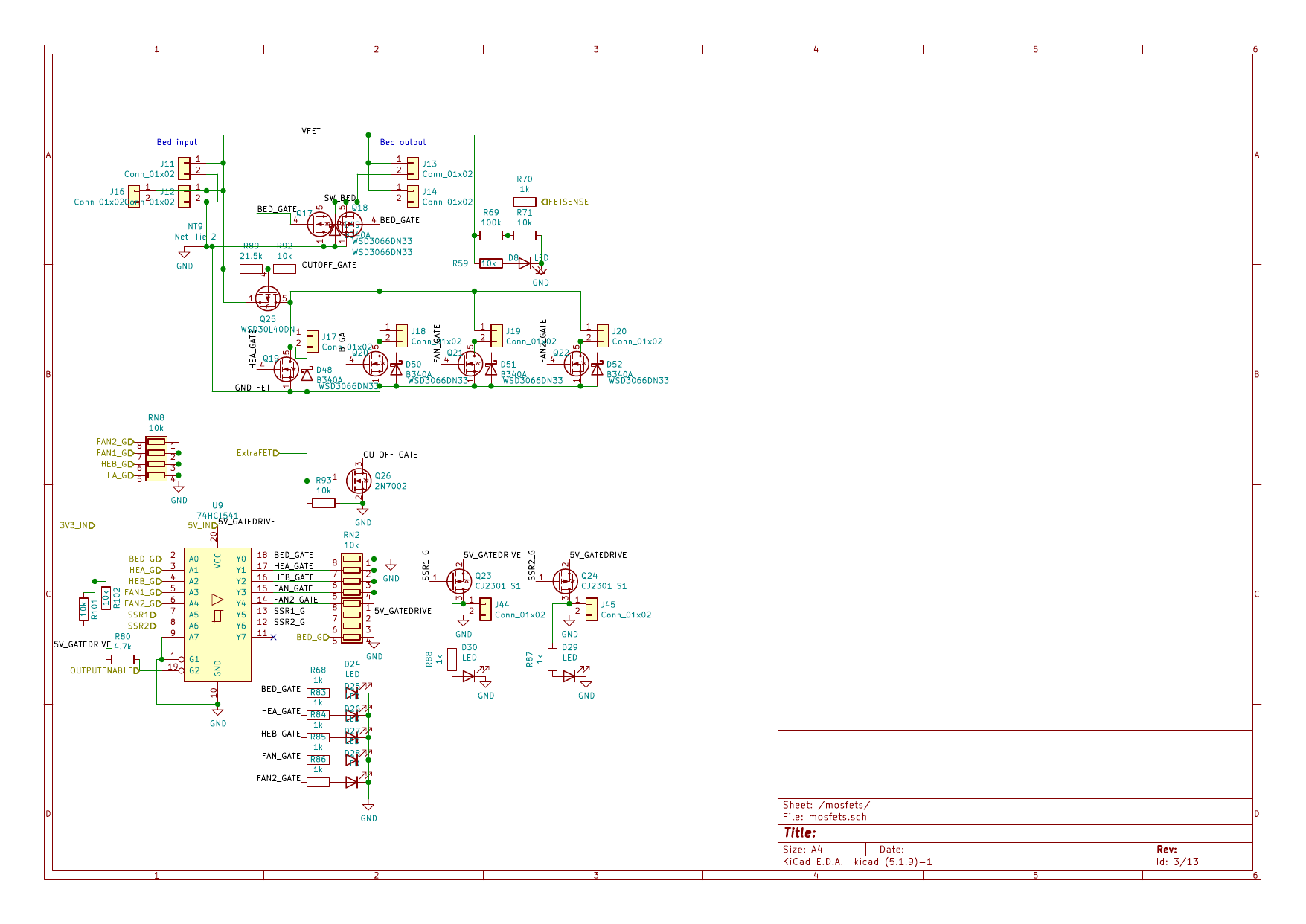
All MOSFET outputs: bed, hotends, fans, and SSR outputs.
Inputs (Page 4)
Thermistor inputs, endstops, and probe input with protection circuitry.
Expansion Headers (Page 5)
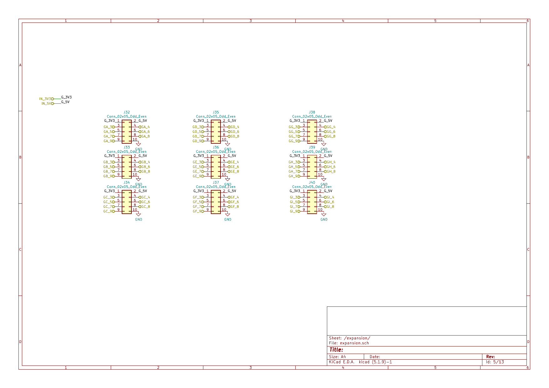
Gadgeteer expansion headers GA through GI.
Power Supply (Page 6)
Main power system: DC-DC converters, voltage regulators, and current limiters.
Ideal Diode Circuits (Pages 7-9)


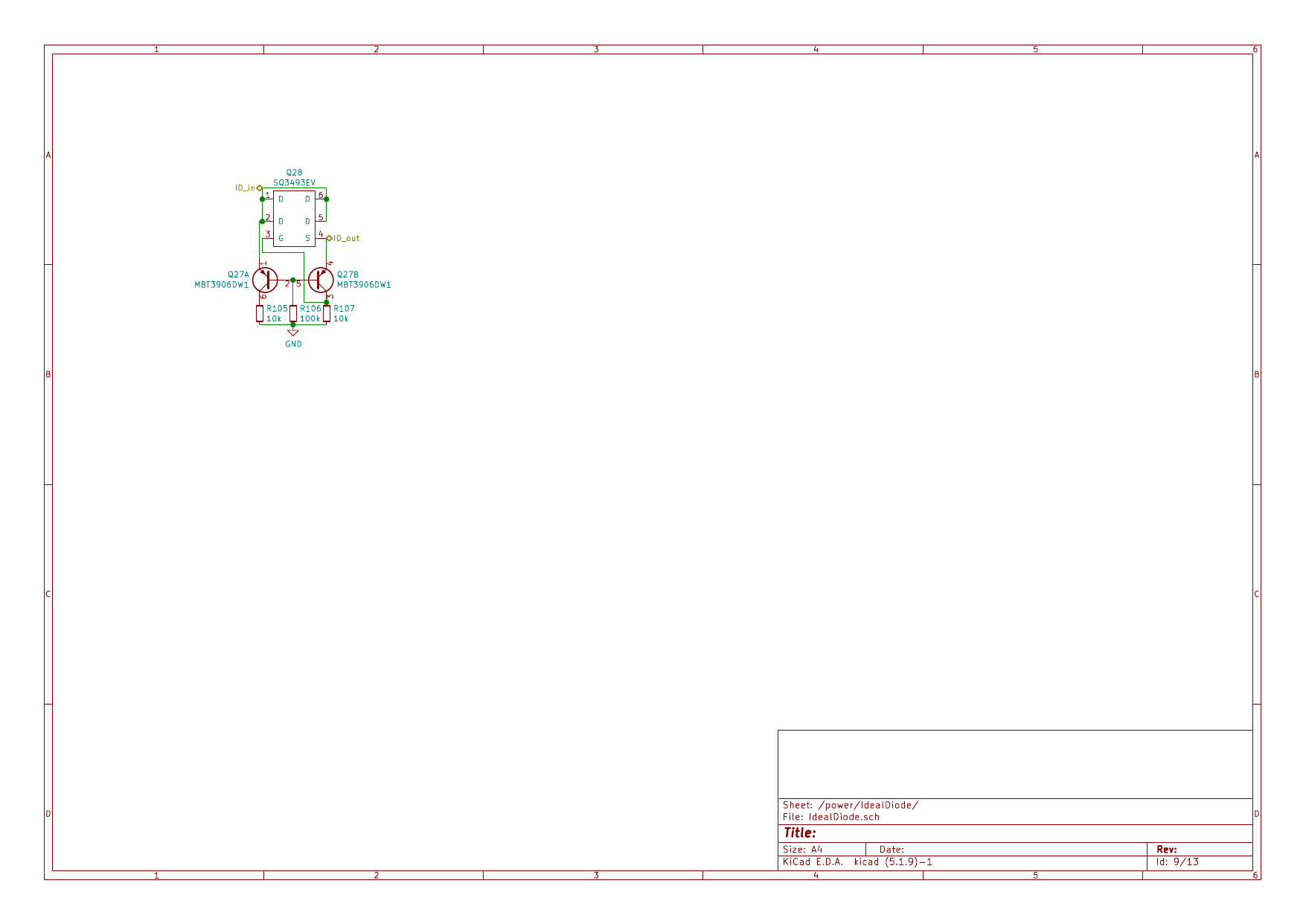
Three identical ideal diode circuits for automatic power source selection.
Motor Drivers (Pages 10-13)


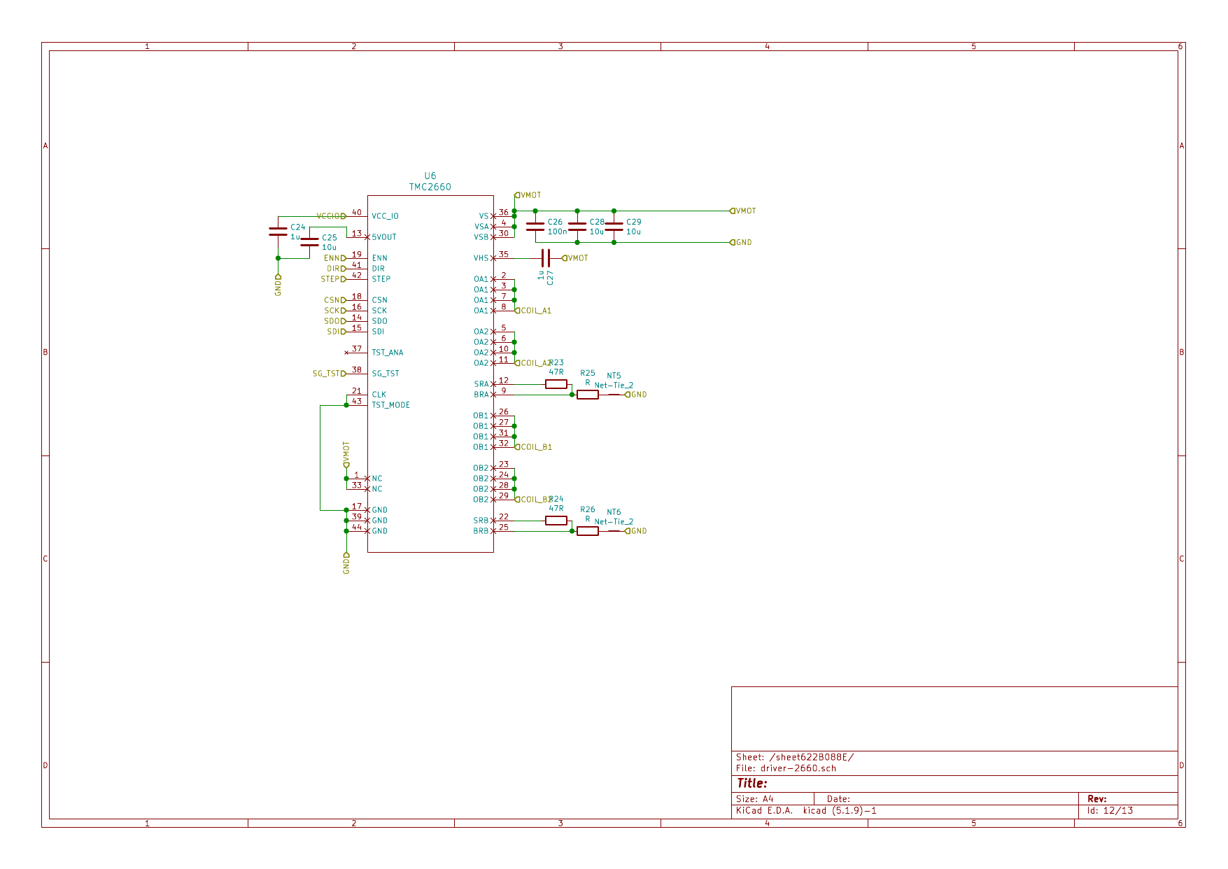

Four identical TMC2660 stepper motor driver circuits (Alpha, Beta, Gamma, Delta).
1. Schematic Sheet Structure
| Sheet | File | Description |
|---|---|---|
| 1/13 | smoothiev2-prime-2660.sch |
Main sheet - MCU, top-level connections |
| 2/13 | ethernet.sch |
Ethernet PHY and RJ45 connector |
| 3/13 | mosfets.sch |
MOSFET outputs for heaters/fans |
| 4/13 | inputs.sch |
Thermistors, endstops, probe inputs |
| 5/13 | expansion.sch |
Gadgeteer expansion headers GA-GI |
| 6/13 | power.sch |
Power supply, DC-DC converters |
| 7/13 | IdealDiode.sch |
Ideal diode circuit (5V regulator) |
| 8/13 | IdealDiode.sch |
Ideal diode circuit (USB) |
| 9/13 | IdealDiode.sch |
Ideal diode circuit (external 5V) |
| 10/13 | driver-2660.sch |
Motor driver A (TMC2660) |
| 11/13 | driver-2660.sch |
Motor driver B (TMC2660) |
| 12/13 | driver-2660.sch |
Motor driver C (TMC2660) |
| 13/13 | driver-2660.sch |
Motor driver D (TMC2660) |
2. Microcontroller (STM32H745XIHx)
STM32H745 MCU
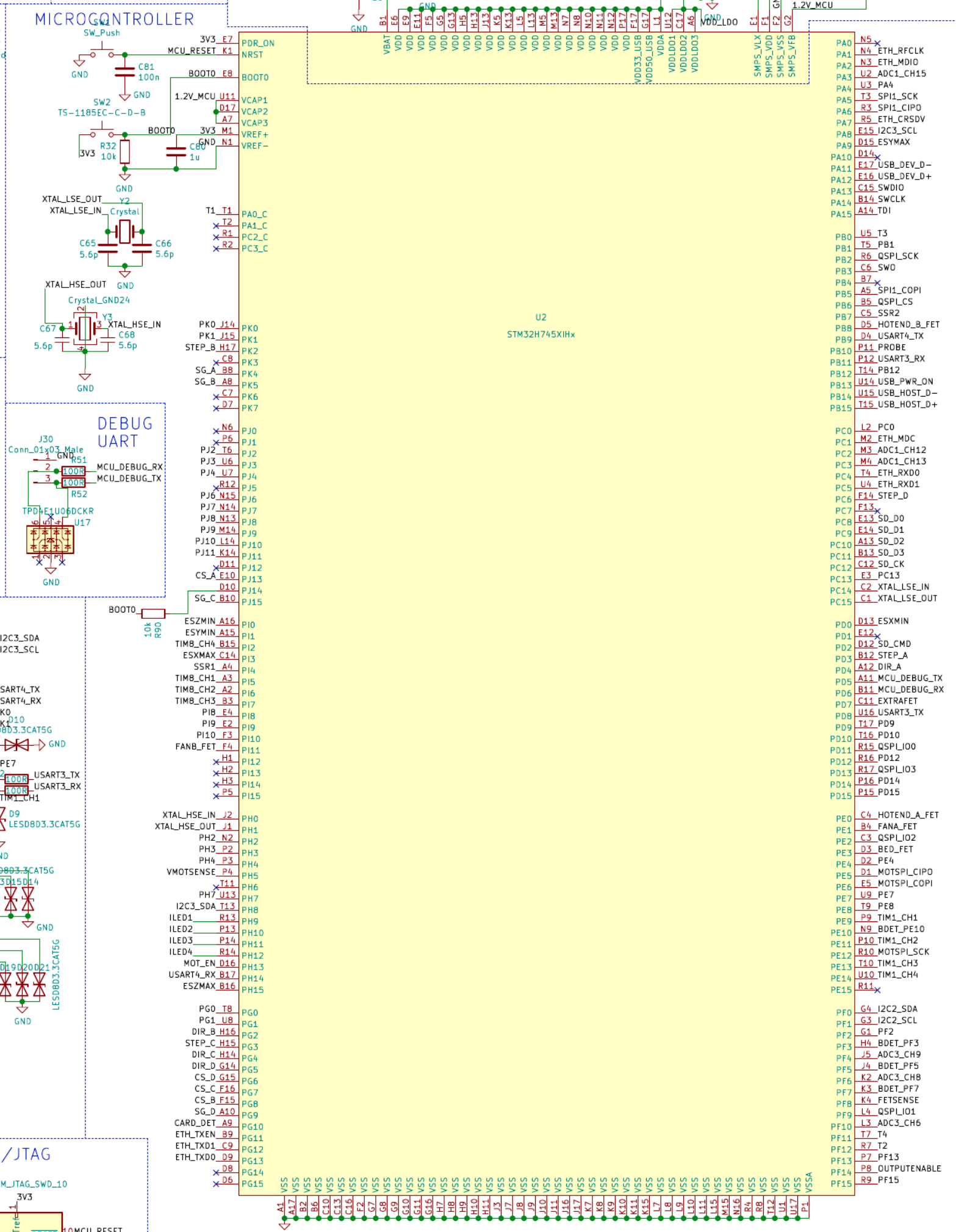
Full STM32H745XIHx BGA265 pinout
Package: 265-pin BGA
Cores: Dual-core Cortex-M7 (480MHz) + Cortex-M4 (240MHz)
Note: M4 core currently unused/disabled in firmware
2.1 Key Pin Assignments
For the complete pin assignment table, see STM32H7 Pin Usage.
Motor Driver SPI Bus:
| Signal | MCU Pin | Function |
|---|---|---|
| MOTSPI_COPI | SPI MOSI to all drivers | |
| MOTSPI_CIPO | SPI MISO from all drivers | |
| MOTSPI_SCK | SPI clock to all drivers |
Motor Chip Selects:
| Driver | MCU Pin | Signal |
|---|---|---|
| Alpha (A) | CS_A | |
| Beta (B) | CS_B | |
| Gamma (C) | CS_C | |
| Delta (D) | CS_D |
Motor Step/Direction:
| Driver | Step Pin | Dir Pin |
|---|---|---|
| Alpha (A) | ||
| Beta (B) | ||
| Gamma (C) | ||
| Delta (D) |
Motor Enable (Shared):
| Signal | MCU Pin | Function |
|---|---|---|
| MOT_EN | Shared enable (active low) |
2.2 Crystal Oscillators
High-Speed External (HSE) - 25MHz:
- Pins:
PH0 (XTAL_HSE_IN),PH1 (XTAL_HSE_OUT) - Component: Y2 (Crystal)
- Load Capacitors: C65, C66 (5.6pF each)
- Purpose: Main system clock source
Low-Speed External (LSE) - 32.768kHz:
- Pins:
PC14 (XTAL_LSE_IN),PC15 (XTAL_LSE_OUT) - Component: Y3 (Crystal_GND24)
- Purpose: RTC clock source
2.3 Debug Interface
SWD/JTAG Connector
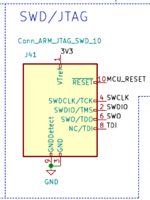
Standard ARM debug connector (J41)
| Signal | MCU Pin | Function |
|---|---|---|
| SWDIO | Debug data | |
| SWCLK | Debug clock | |
| SWO | Trace output | |
| TDI | JTAG data in |
2.4 Debug UART
Debug UART (J30)
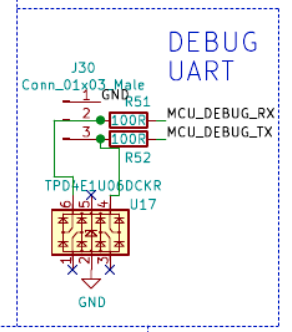
3-pin serial debug header
| Pin | Signal | MCU Pin |
|---|---|---|
| 1 | GND | Ground |
| 2 | RX | |
| 3 | TX |
Baud rate: 115200 8N1
2.5 QSPI Flash
QSPI Flash (AT25SF081)
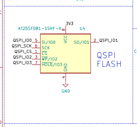
8Mbit Quad-SPI flash for firmware storage
| Signal | MCU Pin | Function |
|---|---|---|
| QSPI_IO0 | Data 0 | |
| QSPI_IO1 | Data 1 | |
| QSPI_IO2 | Data 2 | |
| QSPI_IO3 | Data 3 | |
| QSPI_SCK | Clock | |
| QSPI_CS | Chip select |
2.6 MicroSD and Board Detection
MicroSD + Board Detection
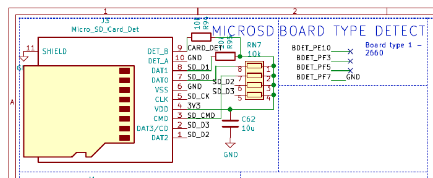
SDIO interface and 4-bit board ID detection
MicroSD (SDIO): High-speed 4-bit interface (10-25 MB/s) vs V1’s SPI (~0.5 MB/s).
Board Detection: 4-bit ID via
3. Power System
5V DC-DC Converter (TPS5430)
VMOT to 5V @ 3A buck converter
3.1 Power Architecture Overview
VMOT (12-24V) ──────┬──► TPS5430 DC-DC ──► 5V (3A) ──┬──► Ideal Diode
                    │                                 │
                    └──► Motor Drivers               └──► MT3410L DC-DC ──► 3.3V (1.2A)

USB 5V ─────────────┬──► MT9700 Current Limit ──► Ideal Diode ──┐
                    │                                            │
                    └──► USB Functions                           ├──► 5V Rail
                                                                 │
External 5V ────────────► MT9700 Current Limit ──► Ideal Diode ──┘
3.2 Main 5V DC-DC Converter (TPS5430DDA)
| Specification | Value |
|---|---|
| Reference | U21 |
| Input | VMOT (12-24V, max 36V) |
| Output | 5V @ 3A continuous |
| Type | Synchronous buck converter |
| Efficiency | ~90% |
| Output Inductor | L3 (22µH) |
| Output Capacitors | C112, C119 (22µF each) |
Disable Jumper:
- JP16: Cut to disable onboard 5V regulator
- Location: Near OSHW logo, top side
3.3 3.3V DC-DC Converter (MT3410L)
3.3V DC-DC (MT3410L)
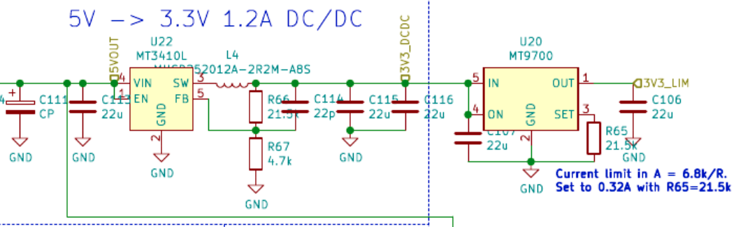
5V to 3.3V @ 1.2A buck converter
| Specification | Value |
|---|---|
| Reference | U22 |
| Input | 5V |
| Output | 3.3V @ 1.2A |
| Output Inductor | L4 (2.2µH) |
3.4 Current-Limited Outputs
| Output | Component | Current Limit | Purpose |
|---|---|---|---|
| 5V_LIM | U19 (MT9700) | 0.32A | Endstops, expansion |
| 3V3_LIM | U20 (MT9700) | 0.32A | Endstops, expansion |
3.5 Ideal Diode Circuits
Ideal Diode Circuit
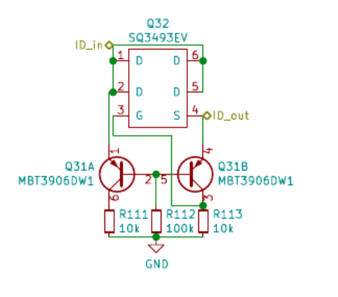
MOSFET-based power source selection
Three identical ideal diode circuits (pages 7-9) enable automatic selection between power sources:
- 5V Regulator Output → 5V rail
- USB 5V → 5V rail (current limited)
- External 5V → 5V rail (current limited)
Uses SQ3493EV dual N-channel MOSFETs with MBT3906DW1 transistor control.
3.6 VMOT Undervoltage Lockout
VMOT Undervoltage Detect
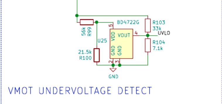
BD4722G voltage detector for motor power monitoring
The UVLO circuit (U25 BD4722G) monitors VMOT and signals the MCU when voltage drops below safe operating threshold. This prevents motor driver damage during brownout conditions.
3.7 External 5V and USB Power
External 5V + USB Current Limiting
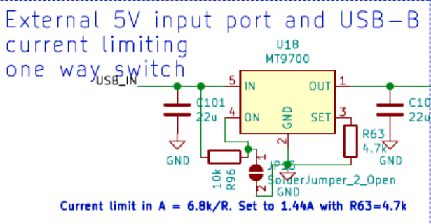
MT9700 current limiters protect external inputs
Both USB 5V and external 5V inputs are protected by MT9700 current limiting switches:
- USB 5V (U18): Limited to 1.44A (R63=4.7k)
- External 5V (J10): Limited to 0.32A (R65=21.5k)
3.8 RTC Backup Battery
RTC Backup Battery
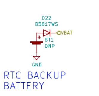
CR2032 battery holder for RTC timekeeping
A CR2032 coin cell (B5817WS holder) maintains RTC time when main power is off.
3.9 Power Connectors
| Connector | Type | Pins | Function |
|---|---|---|---|
| J5 | Screw Terminal | 4 | VMOT input |
| J6 | Screw Terminal | 4 | VFET input 1 |
| J7 | Screw Terminal | 4 | VFET input 2 |
| J8 | Screw Terminal | 4 | VMOT input (alternate) |
| J10 | Conn_01x02 | 2 | External 5V input |
3.10 Complete Power System
Full Power System Schematic
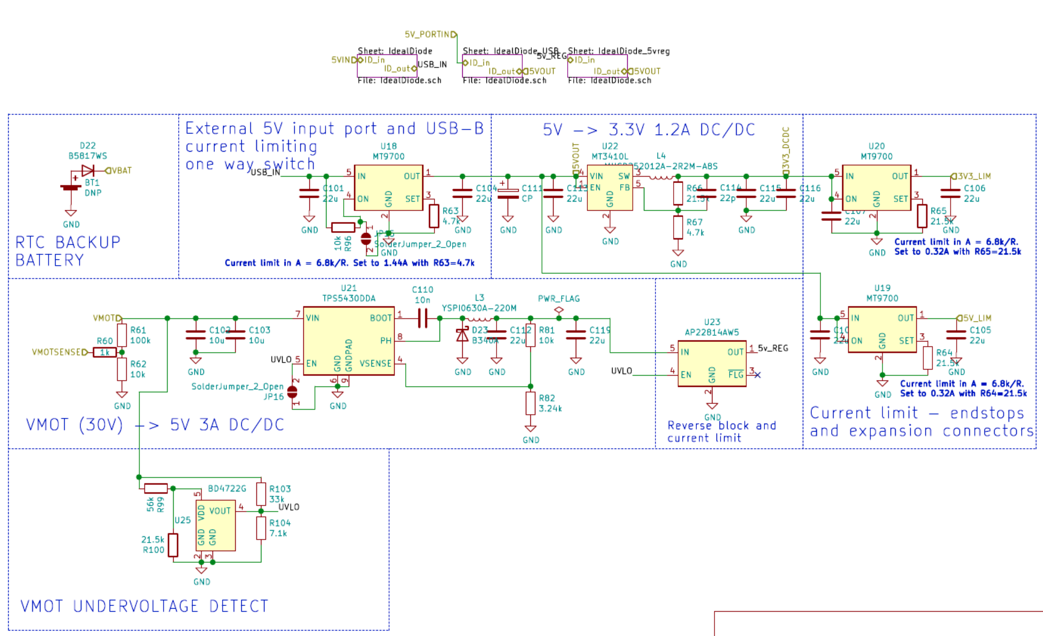
Complete power supply schematic showing all regulators, current limiters, and power distribution
4. Motor Drivers (TMC2660)
Motor Driver Blocks (Main Sheet)
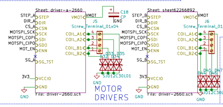
Hierarchical block showing drivers A/B with shared SPI bus
Motor Driver Blocks C/D
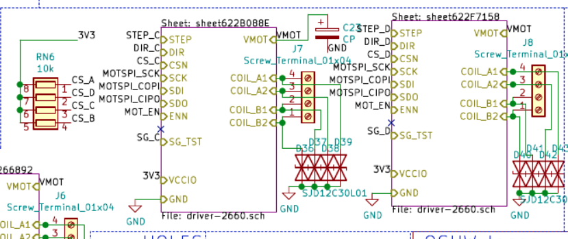
Hierarchical block showing drivers C/D (Gamma/Delta)
TMC2660 Driver Circuit
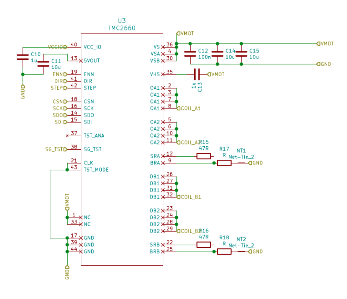
Each of the 4 motor drivers uses this circuit
4.1 Driver Overview
| Driver | Reference | Sheet | Axis |
|---|---|---|---|
| A | U3 | 10/13 | Alpha (X) |
| B | U5 | 11/13 | Beta (Y) |
| C | U6 | 12/13 | Gamma (Z) |
| D | U7 | 13/13 | Delta (E) |
4.2 TMC2660 Specifications
| Specification | Value |
|---|---|
| Package | 44-pin QFN |
| Motor Current | Up to 2.8A peak (1.2-2.2A ideal) |
| Motor Voltage | Up to 30V |
| Microstepping | Up to 1/256 |
| Interface | SPI for configuration |
Features:
- StealthChop2 (silent operation)
- SpreadCycle (high performance)
- StallGuard4 (sensorless homing)
- CoolStep (dynamic current)
4.3 Current Sense Resistors
| Driver | Resistors | Notes |
|---|---|---|
| A | R17, R18 | Set at assembly |
| B | R21, R22 | Set at assembly |
| C | R25, R26 | Set at assembly |
| D | R29, R30 | Set at assembly |
Current Calculation:
- Peak current = 0.165V / R_sense
- For 0.1Ω: I_peak = 1.65A
- For 0.05Ω: I_peak = 3.3A
4.4 StallGuard Outputs
| Driver | MCU Pin | Signal |
|---|---|---|
| A | SG_TST_A | |
| B | SG_TST_B | |
| C | SG_TST_C | |
| D | SG_TST_D |
5. MOSFET Outputs
MOSFETs Block (Main Sheet)
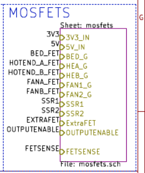
Hierarchical block showing all MOSFET output signals
MOSFET Gate Driver (74HCT541)
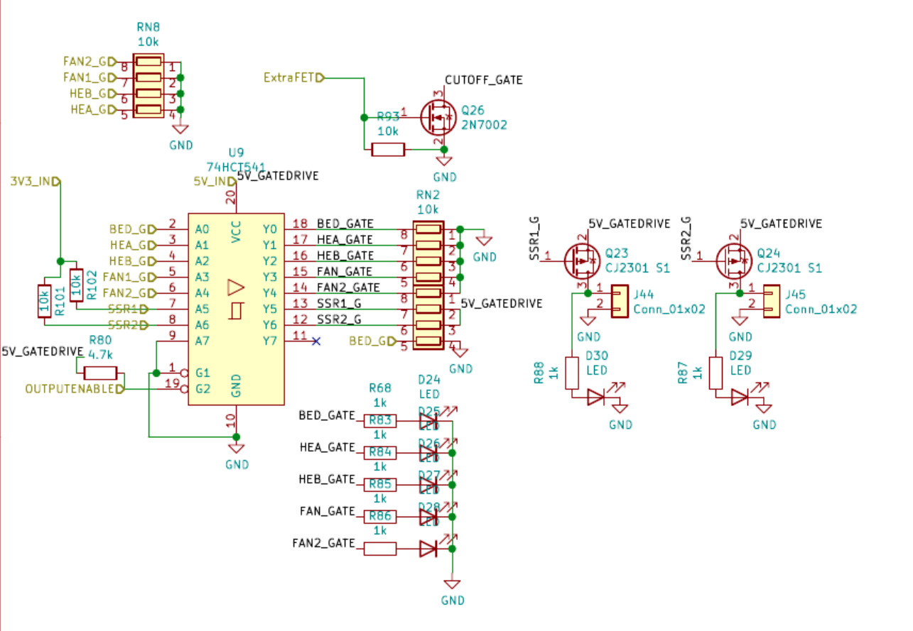
Buffer IC with master output enable control
5.1 Output Summary
| Output | MOSFET | Current | LED | MCU Signal |
|---|---|---|---|---|
| Bed | 2x WSD30L40DN (parallel) | ~10-12A | D25 | BED_G |
| Hotend A | WSD3066DN | ~5A | D26 | HEA_G ( |
| Hotend B | WSD3066DN | ~5A | D27 | HEB_G ( |
| Fan 1 | WSD3066DN | ~5A | D28 | FAN1_G ( |
| Fan 2 | WSD3066DN | ~5A | D29, D30 | FAN2_G ( |
| SSR1 | CJ2301 S1 | Signal | D24 | |
| SSR2 | CJ2301 S1 | Signal | - | |
| ExtraFET | Via buffer | - | - |
5.2 Safety System
Safety Cutoff Circuit
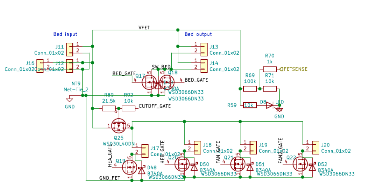
High-side PFET cutoff for hotends and fans
74HCT541 Buffer (U9):
- Buffers MCU signals to MOSFET gates
- OUTPUTENABLE signal provides master control (
PJ5 )
5.3 VFET Voltage Monitoring
| Signal | Components | Divider Ratio |
|---|---|---|
| FETSENSE | R69 (100k), R70 (1k), R71 (10k) | 11:1 |
5.4 Complete MOSFET Schematic
Full MOSFET Output Schematic
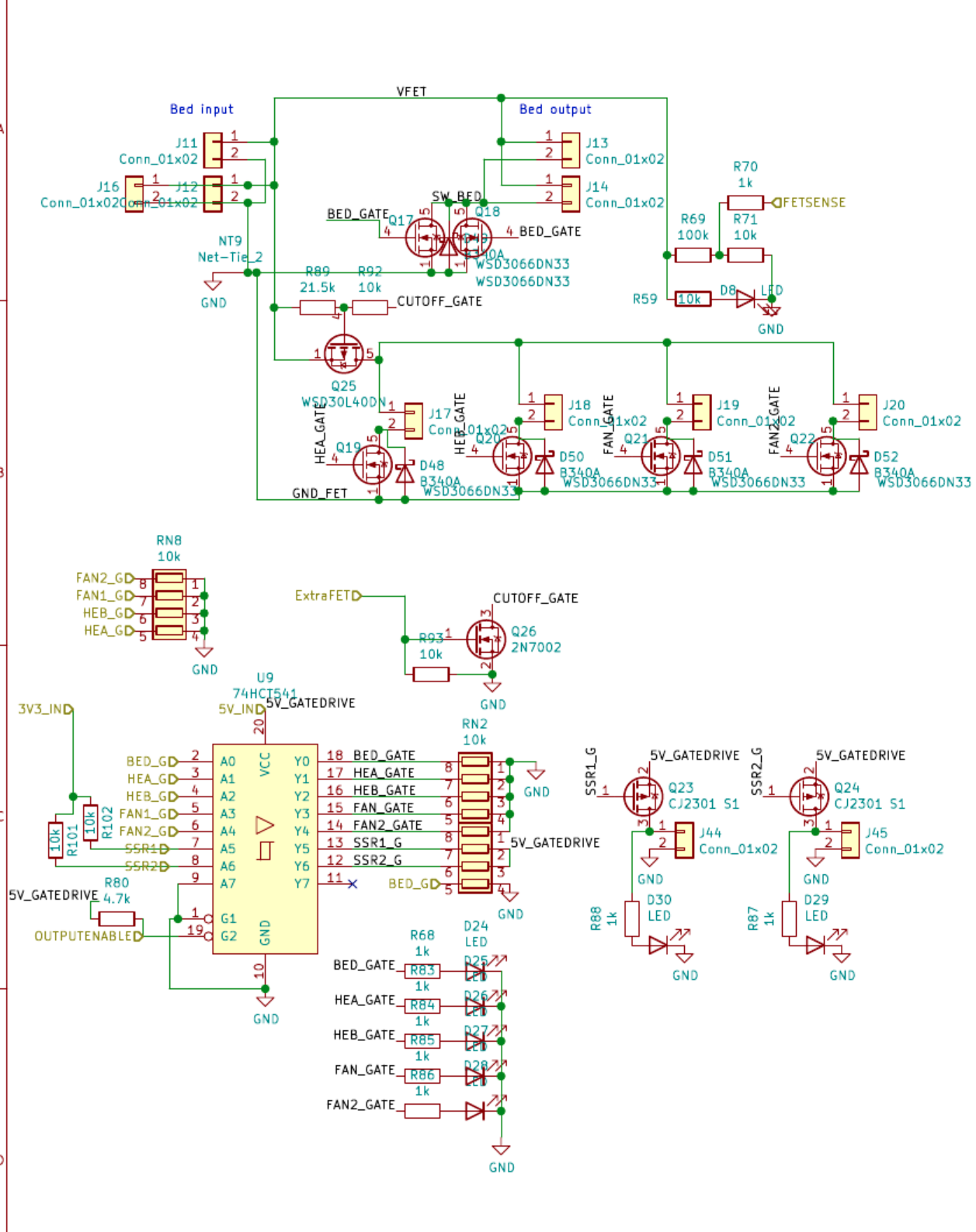
Complete MOSFET output schematic showing bed, hotends, fans, SSR outputs, and safety cutoff
6. Inputs
Inputs Block (Main Sheet)
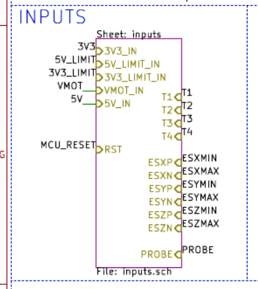
Hierarchical block showing all input signals
6.1 Thermistor Inputs
Thermistor Buffer Circuit
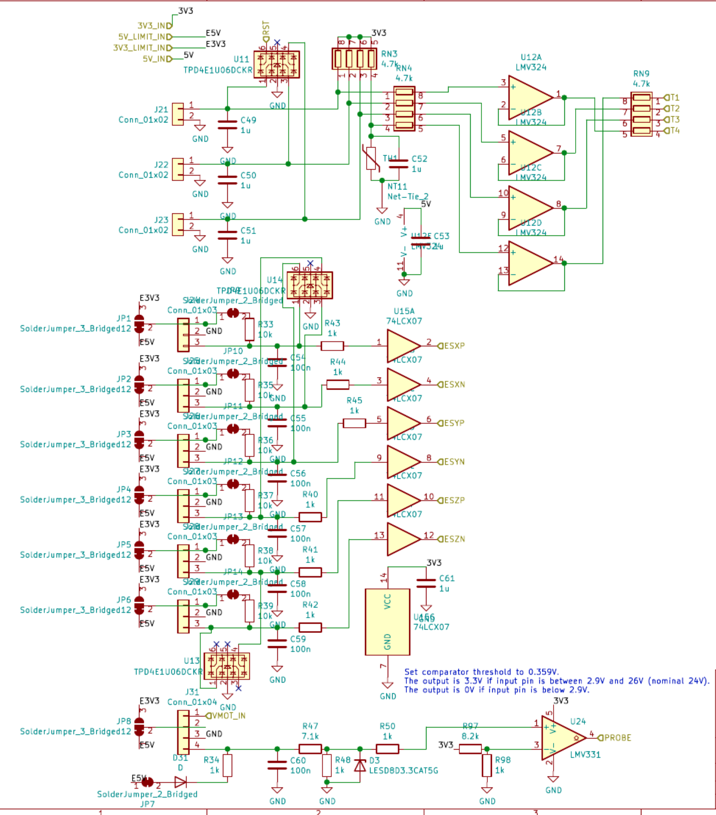
4 buffered thermistor inputs via LMV324 op-amp
| Channel | Op-Amp | Connector | MCU Pin | ADC |
|---|---|---|---|---|
| T1 | U12A | J25 | ADC1_INP16 | |
| T2 | U12B | J24 | ADC1_INP17 | |
| T3 | U12C | J26 | ADC3_INP0 | |
| T4 | U12D | J27-J29 | ADC3_INP1 |
Note: The _C suffix pins are STM32 hardware names for dedicated analog inputs. In config files, use ADC format: ADC1_0, ADC1_1, ADC1_2, ADC1_3
6.2 Endstop Inputs
Endstop Input Circuit
6 endstops with ESD protection and pull configuration
| Endstop | MCU Pin | Connector |
|---|---|---|
| X Min | - | |
| X Max | - | |
| Y Min | - | |
| Y Max | - | |
| Z Min | - | |
| Z Max | - |
All endstops are buffered and ESD protected.
6.3 Probe Input
Probe Input Circuit
Comparator-based probe input with JP7 voltage range selector
- JP7 Intact (default): For probes <5V (BLTouch, mechanical switches)
- JP7 Cut: REQUIRED for probes >5V (inductive, capacitive, up to 45V)
| Specification | Value |
|---|---|
| MCU Pin | |
| Input Type | Comparator-based |
| Voltage Range | 3-45V (configurable via JP7) |
| Protection | ESD + buffering + comparator |
7. Expansion Headers (Gadgeteer)
Expansion Headers Schematic
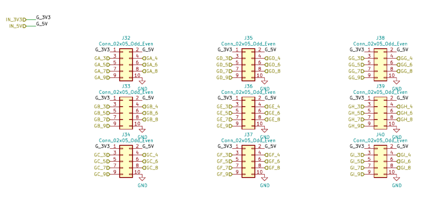
9 Gadgeteer-style 10-pin expansion headers
7.1 Header Overview
| Header | Pins 3-9 Functions | Special Features |
|---|---|---|
| GA | GPIO | Motor SPI, encoder |
| GB | GPIO | General GPIO |
| GC | GPIO | General GPIO |
| GD | UART4 (PD0 RX, PD1 TX), GPIO | Serial communication |
| GE | TIM15 PWM (PE5 CH1, PE6 CH2), GPIO | PWM outputs |
| GF | GPIO | General GPIO |
| GG | I2C4 (PF14 SCL, PF15 SDA), GPIO | I2C bus |
| GH | ADC capable, GPIO | Analog inputs |
| GI | GPIO | General GPIO |
7.2 Standard Pinout (All Headers)
| Pin | Function |
|---|---|
| 1-7 | GPIO (varies by header) |
| 8 | 5V |
| 9 | 3.3V |
| 10 | GND |
7.3 MCU-Side Connections
Expansion Headers MCU Side
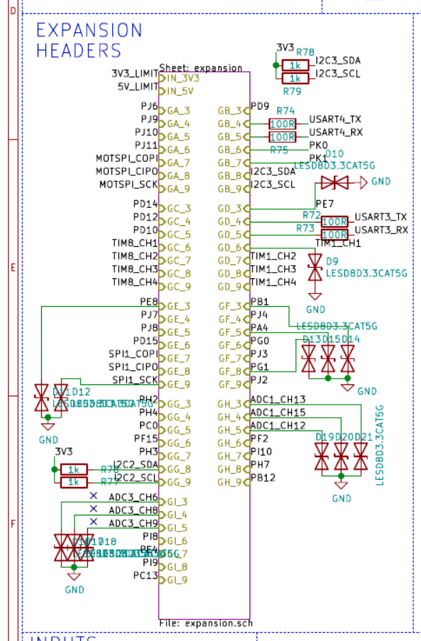
MCU pin assignments for all expansion headers
The expansion headers connect to dedicated GPIO banks on the MCU, with some headers providing special peripheral functions:
- GD: UART4 for serial communication
- GE: TIM15 for PWM output
- GG: I2C4 for sensor/display buses
- GH: ADC channels for analog input
8. USB
USB Host + Device Circuit
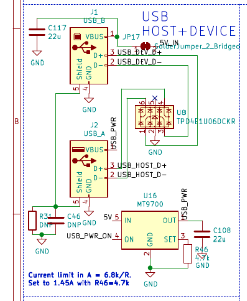
USB-B device and SD card interface
8.1 USB Device
| Signal | MCU Pin |
|---|---|
| USB_DEV_D- | |
| USB_DEV_D+ |
8.2 USB Host (Hardware Present)
| Signal | MCU Pin |
|---|---|
| USB_HOST_D- | |
| USB_HOST_D+ | |
| USB_PWR_ON |
9. Ethernet
Ethernet Block (Main Sheet)
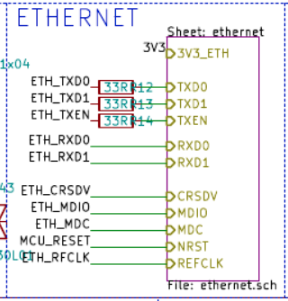
Hierarchical block showing Ethernet signals
Ethernet PHY (LAN8720A)
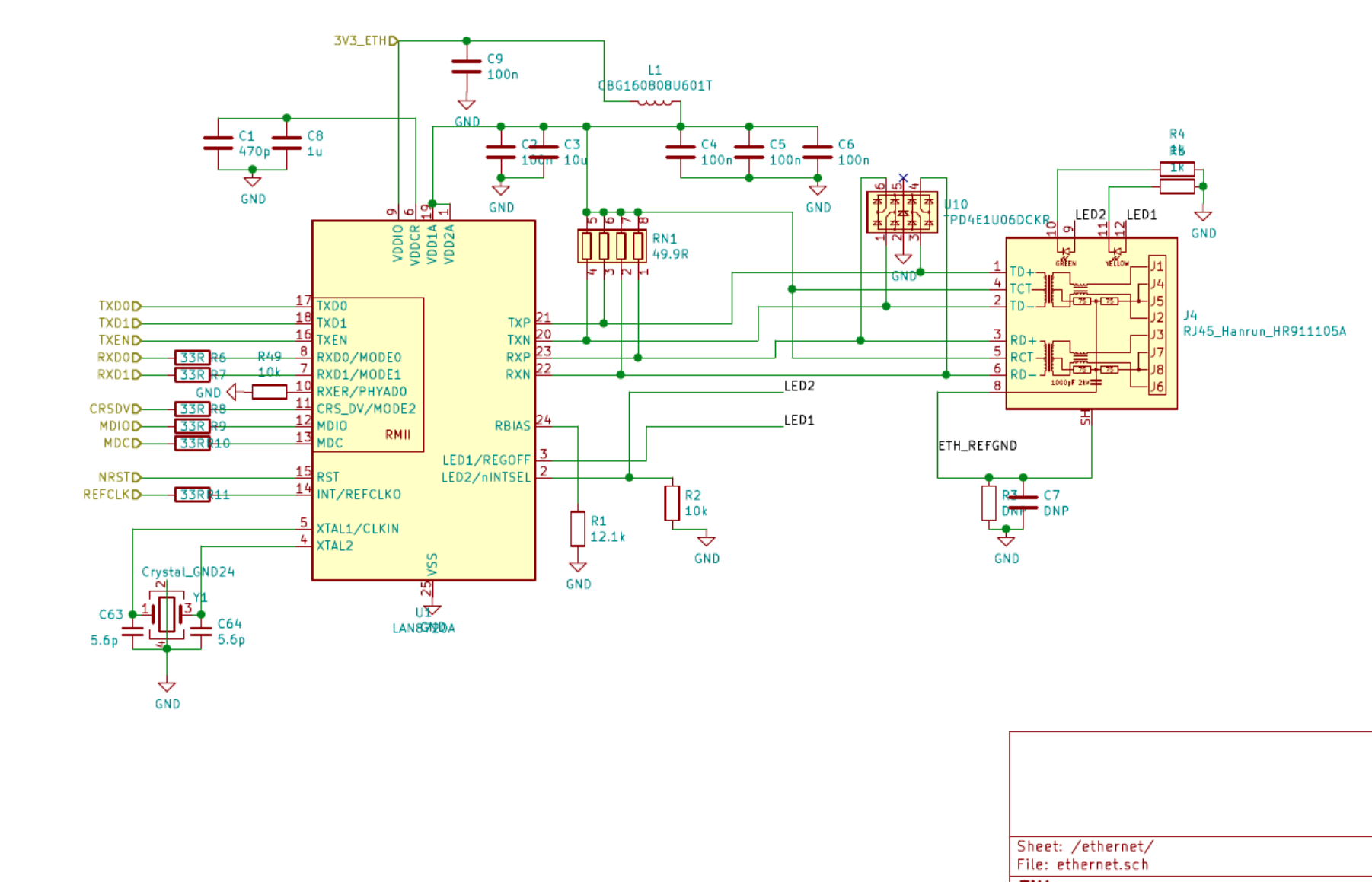
Complete Ethernet interface with integrated magnetics RJ45
9.1 LAN8720A PHY
| Specification | Value |
|---|---|
| Part | LAN8720A |
| Interface | RMII (Reduced MII) |
| Speed | 10/100 Mbps |
| Features | Auto-MDIX, Auto-negotiation |
9.2 RMII Signals
| Signal | MCU Pin | Function |
|---|---|---|
| ETH_TXD0 | Transmit data 0 | |
| ETH_TXD1 | Transmit data 1 | |
| ETH_TXEN | Transmit enable | |
| ETH_RXD0 | Receive data 0 | |
| ETH_RXD1 | Receive data 1 | |
| ETH_CRSDV | Carrier sense/data valid | |
| ETH_MDIO | Management data I/O | |
| ETH_MDC | Management data clock | |
| ETH_REFCLK | 50MHz reference clock |
9.3 RJ45 Connector
The board uses an RJ45 connector with integrated magnetics (HR911105A), including link and activity LEDs.
10. Board Detection
The board automatically detects its type via 4 board ID pins:
| Pin | MCU Pin | Function |
|---|---|---|
| BDET_PF3 | Board detect bit 0 | |
| BDET_PF5 | Board detect bit 1 | |
| BDET_PF7 | Board detect bit 2 | |
| BDET_PE10 | Board detect bit 3 |
- Board ID 0: TMC2590 drivers
- Board ID 1: TMC2660 drivers
10. LED Indicators
Debug LED Circuit
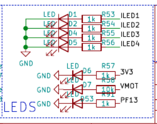
4 debug LEDs showing boot progress
10.1 Debug LEDs
| LED | MCU Pin | Phase |
|---|---|---|
| ILED1 | Phase 4 | |
| ILED2 | Phase 3 | |
| ILED3 | Phase 2 | |
| ILED4 | Phase 1 |
Boot Sequence:
- LED 4: HAL, UART, RTC, board ID
- LED 3: Tickers creation
- LED 2: Module configuration
- LED 1: Ticker startup, ADC
- All on: Boot complete
10.2 Other LEDs
| LED | Function |
|---|---|
| MSD LED | Mass Storage mode ( |
| Vmot LED | Motor power present |
| Vfet LED | MOSFET power present |
| 3.3V LED | Logic power present |
| Per-MOSFET LEDs | Output state |
12. Mounting Holes
PCB Mounting Holes
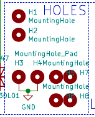
4 mounting holes (H1-H4) with grounding pads
The board includes four M3 mounting holes at standard locations. Holes H3 and H4 include grounding pads for chassis connection.
Related Pages
- Smoothieboard V2 Prime - Technical specifications
- STM32H7 Pin Usage - Complete pin assignments
- Smoothieboard V2 Differences - V1 vs V2 comparison
- Pin Configuration - How to configure pins
Last updated: November 2025