This page documents all pin assignments for the STM32H745XIHx microcontroller on Smoothieboard V2 Prime.
This comprehensive reference shows how every pin on the STM32H745 is assigned on Smoothieboard V2 Prime (TMC2660 variant). Use this to identify available pins for custom functionality via the Gadgeteer expansion headers.
Pin List
The following table shows all pin assignments on the STM32H745XIHx microcontroller:
STM32 Pin
Smoothie Pin
BGA Position
Assignment
Comment
PA0
PA0
N5
GPIO
General purpose
PA0_C
ADC1_0
N5
Board Temp (T4)
Config: ADC1_0, buffered via LMV324
PA1
PA1
N4
ETH_REFCLK
50MHz Ethernet reference clock
PF11
ADC1_1
P5
Thermistor 1 (T1)
Config: ADC1_1, buffered via LMV324
PF12
ADC1_2
R7
Thermistor 2 (T2)
Config: ADC1_2, buffered via LMV324
PA2
PA2
N3
ETH_MDIO
Ethernet management data I/O
PA3
PA3
U2
Expansion GH
ADC1_CH15 available
PA4
PA4
U3
I2C2_SCL
User I2C bus clock
PA5
PA5
T3
Expansion GH
DAC1_OUT2 available
PA6
PA6
R3
Expansion GH
ADC1_CH3 available
PA7
PA7
R5
ETH_CRSDV
Ethernet carrier sense/data valid
PA8
PA8
E15
Expansion GH
GPIO
PA9
PA9
D15
Expansion GH
GPIO
PA10
PA10
D14
Expansion GI
GPIO
PA11
PA11
E17
USB_DEV_D-
USB device data minus
PA12
PA12
E16
USB_DEV_D+
USB device data plus
PA13
PA13
C15
SWDIO
Debug data (hardcoded)
PA14
PA14
B14
SWCLK
Debug clock (hardcoded)
PA15
PA15
A14
TDI
JTAG data in
PB0
PB0
U5
PROBE
Probe input via comparator
PB1
PB1
T5
I2C2_SDA
User I2C bus data
PB2
PB2
R6
QSPI_SCK
QSPI flash clock
PB3
PB3
C6
SPI1_SCK / SWO
User SPI clock / trace output
PB4
PB4
B7
SPI1_MISO
User SPI data in
PB5
PB5
A5
SPI1_MOSI
User SPI data out
PB6
PB6
B5
QSPI_CS
QSPI flash chip select
PB7
PB7
C5
GPIO
General purpose
PB8
PB8
D5
GPIO
General purpose
PB9
PB9
D4
GPIO
General purpose
PB10
PB10
P11
Expansion GI
GPIO
PB11
PB11
P12
Expansion GI
GPIO
PB12
PB12
T14
Motor B CS
TMC2660 chip select
PB13
PB13
U14
USB_PWR_ON
USB host power control
PB14
PB14
U15
USB_HOST_D+
USB host data plus
PB15
PB15
T15
USB_HOST_D-
USB host data minus
PC0
PC0
L2
SSR1
Solid state relay output 1
PC1
PC1
M2
ETH_MDC
Ethernet management clock
PC2
PC2
M3
Expansion (GH)
ADC1_4 available as ADC1_4
PC3
PC3
M4
Expansion (GH)
ADC1_5 available as ADC1_5
PC4
PC4
T4
VMOT_SENSE
Motor voltage sense (11:1 divider)
PC5
PC5
U4
VFET_SENSE
MOSFET voltage sense (11:1 divider)
PC6
PC6
F14
Expansion GC
GPIO
PC7
PC7
F13
Expansion GC
GPIO
PC8
PC8
E13
SD_D0
SD card data 0 (hardcoded)
PC9
PC9
E14
SD_D1
SD card data 1 (hardcoded)
PC10
PC10
A13
SD_D2
SD card data 2 (hardcoded)
PC11
PC11
B13
SD_D3
SD card data 3 (hardcoded)
PC12
PC12
C12
SD_CK
SD card clock (hardcoded)
PC13
PC13
E3
GPIO
General purpose
PC14
PC14
C2
XTAL_LSE_IN
32.768kHz crystal in (hardcoded)
PC15
PC15
C1
XTAL_LSE_OUT
32.768kHz crystal out (hardcoded)
PD0
PD0
D13
UART4_RX
Expansion GD UART receive
PD1
PD1
E12
UART4_TX
Expansion GD UART transmit
PD2
PD2
D12
SD_CMD
SD card command (hardcoded)
PD3
PD3
B12
Expansion GD
GPIO
PD4
PD4
A12
Expansion GD
GPIO
PD5
PD5
A11
USART2_TX / Debug TX
Debug UART transmit
PD6
PD6
B11
USART2_RX / Debug RX
Debug UART receive
PD7
PD7
C11
Expansion GD
GPIO
PD8
PD8
U16
USART3_TX
Expansion UART transmit
PD9
PD9
T17
USART3_RX
Expansion UART receive
PD10
PD10
T16
GPIO
General purpose
PD11
PD11
R15
QSPI_IO0
QSPI flash data 0
PD12
PD12
R16
QSPI_IO1
QSPI flash data 1
PD13
PD13
R17
QSPI_IO3
QSPI flash data 3
PD14
PD14
P16
MOTSPI_MOSI
Motor SPI data out (hardcoded)
PD15
PD15
P15
Expansion GC
GPIO
PE0
PE0
C4
Expansion GE
GPIO
PE1
PE1
B4
Expansion GE
GPIO
PE2
PE2
C3
QSPI_IO2
QSPI flash data 2
PE3
PE3
D3
Expansion GE
GPIO
PE4
PE4
D2
MOTSPI_MISO
Motor SPI data in (hardcoded)
PE5
PE5
D1
TIM15_CH1
Expansion GE PWM
PE6
PE6
E5
TIM15_CH2
Expansion GE PWM
PE7
PE7
U9
Expansion GE
GPIO
PE8
PE8
T9
Expansion GE
GPIO
PE9
PE9
P9
TIM1_CH1
Timer 1 channel 1 PWM
PE10
PE10
N9
Motor D Step / BDET
Motor D step, also board detect bit 3
PE11
PE11
P10
TIM1_CH2
Timer 1 channel 2 PWM
PE12
PE12
R10
Motor D Dir / TIM1_CH3
Motor D direction
PE13
PE13
T10
TIM1_CH4
Timer 1 channel 4 PWM (spare)
PE14
PE14
U10
Motor C Step
TMC2660 motor C step
PE15
PE15
R11
Motor C Dir
TMC2660 motor C direction
PF0
PF0
G4
Expansion GF
GPIO
PF1
PF1
G3
Expansion GF
GPIO
PF2
PF2
G1
Expansion GF
GPIO
PF3
PF3
H4
BDET_PF3
Board detect bit 0 (hardcoded)
PF4
PF4
J5
Expansion GF
GPIO
PF5
PF5
J4
BDET_PF5
Board detect bit 1 (hardcoded)
PF6
PF6
K2
Expansion GF
GPIO
PF7
PF7
K3
BDET_PF7
Board detect bit 2 (hardcoded)
PF8
PF8
K4
Expansion GF
GPIO
PF9
PF9
L4
Expansion GF
GPIO
PF10
PF10
L3
Expansion GG
GPIO
PF11
PF11
T7
Motor B Dir
TMC2660 motor B direction
PF12
PF12
R7
Motor B Step
TMC2660 motor B step
PF13
PF13
P7
Expansion GG
GPIO
PF14
PF14
P8
I2C4_SCL
Expansion GG I2C clock
PF15
PF15
R9
I2C4_SDA
Expansion GG I2C data
PG0
PG0
T8
Motor A Step
TMC2660 motor A step
PG1
PG1
U8
Motor A Dir
TMC2660 motor A direction
PG2
PG2
H16
CARD_DET
SD card detection
PG3
PG3
H15
Expansion GB
GPIO
PG4
PG4
H14
Expansion GB
GPIO
PG5
PG5
G14
Expansion GB
GPIO
PG6
PG6
G15
Expansion GC
GPIO
PG7
PG7
F16
Expansion GC
GPIO
PG8
PG8
F15
Expansion GC
GPIO
PG9
PG9
A10
ESXMAX
X max endstop
PG10
PG10
A9
ESXMIN
X min endstop
PG11
PG11
B9
ESYMIN
Y min endstop
PG12
PG12
C9
ESYMAX
Y max endstop
PG13
PG13
D9
ESZMIN
Z min endstop
PG14
PG14
D8
ESZMAX
Z max endstop
PG15
PG15
D6
GPIO
General purpose
PH0
PH0
J2
XTAL_HSE_IN
25MHz crystal in (hardcoded)
PH1
PH1
J1
XTAL_HSE_OUT
25MHz crystal out (hardcoded)
PH2
PH2
N2
ExtraFET
Extra switched output
PH3
PH3
P2
Expansion GG
GPIO
PH4
PH4
P3
Expansion GG
GPIO
PH5
PH5
P4
Expansion GG
GPIO
PH6
PH6
T11
TIM8_CH1
Timer 8 channel 1 PWM
PH7
PH7
U13
TIM8_CH4 / I2C3_SCL
Timer 8 ch4 / I2C3 clock
PH8
PH8
T13
TIM8_CH2 / I2C3_SDA
Timer 8 ch2 / I2C3 data
PH9
PH9
R13
TIM8_CH3
Timer 8 channel 3 PWM
PH10
PH10
P13
Expansion GI
GPIO
PH11
PH11
P14
Expansion GI
GPIO
PH12
PH12
R14
Expansion GI
GPIO
PH13
PH13
D16
MOT_EN
Motor enable (shared, active low)
PH14
PH14
B17
Expansion GI
GPIO
PH15
PH15
B16
GPIO
General purpose
PI0
PI0
A16
MSD LED
Mass storage mode indicator
PI1
PI1
A15
GPIO
General purpose
PI2
PI2
B15
GPIO
General purpose
PI3
PI3
C14
GPIO
General purpose
PI4
PI4
A4
GPIO
General purpose
PI5
PI5
A3
GPIO
General purpose
PI6
PI6
A2
GPIO
General purpose
PI7
PI7
B3
GPIO
General purpose
PI8
PI8
E4
GPIO
General purpose
PI9
PI9
E2
GPIO
General purpose
PI10
PI10
F3
MOTSPI_SCK
Motor SPI clock (hardcoded)
PI11
PI11
F4
Expansion GA
GPIO
PI12
PI12
H1
Expansion GA
GPIO
PI13
PI13
H2
Expansion GA
GPIO
PI14
PI14
H3
Expansion GA
GPIO
PI15
PI15
P5
Expansion GA
GPIO
PJ0
PJ0
N6
Expansion GA
GPIO
PJ1
PJ1
P6
Expansion GA
GPIO
PJ2
PJ2
T6
Motor A CS
TMC2660 motor A chip select
PJ3
PJ3
U6
Motor C CS
TMC2660 motor C chip select
PJ4
PJ4
U7
Motor D CS
TMC2660 motor D chip select
PJ5
PJ5
R12
OUTPUTENABLE
Master FET output enable
PJ6
PJ6
N15
HEA_G
Hotend A MOSFET gate
PJ7
PJ7
N14
HEB_G
Hotend B MOSFET gate
PJ8
PJ8
N13
FAN1_G
Fan 1 MOSFET gate
PJ9
PJ9
M14
FAN2_G
Fan 2 MOSFET gate
PJ10
PJ10
L14
BED_G
Bed MOSFET gate
PJ11
PJ11
K14
SSR2
Solid state relay output 2
PJ12
PJ12
D11
ILED3
Debug LED 3
PJ13
PJ13
E10
ILED2
Debug LED 2
PJ14
PJ14
D10
ILED1
Debug LED 1
PJ15
PJ15
B10
ILED4
Debug LED 4
PK0
PK0
J14
SG_TST_A
Motor A StallGuard output
PK1
PK1
J15
SG_TST_B
Motor B StallGuard output
PK2
PK2
H17
SG_TST_C
Motor C StallGuard output
PK3
PK3
C8
SG_TST_D
Motor D StallGuard output
PK4
PK4
B8
Expansion GB
GPIO
PK5
PK5
A8
Expansion GB
GPIO
PK6
PK6
C7
Expansion GB
GPIO
PK7
PK7
D7
Expansion GB
GPIO
BOOT0
BOOT0
E8
BOOT0
Boot mode (LOW=flash, HIGH=DFU)
NRST
NRST
K1
MCU_RESET
System reset (active low)
Hardwired Pins:
The following pins are hardwired and would need source code changes to modify:
USB Device: PA11, PA12
Debug (SWD): PA13 (SWDIO), PA14 (SWCLK)
SD Card (SDIO): PC8-PC12, PD2
Crystals: PH0, PH1 (HSE), PC14, PC15 (LSE)
Motor SPI: PD14 (MOSI), PE4 (MISO), PI10 (SCK)
Board detect: PF3, PF5, PF7, PE10
All other pins can be reassigned via the configuration file.
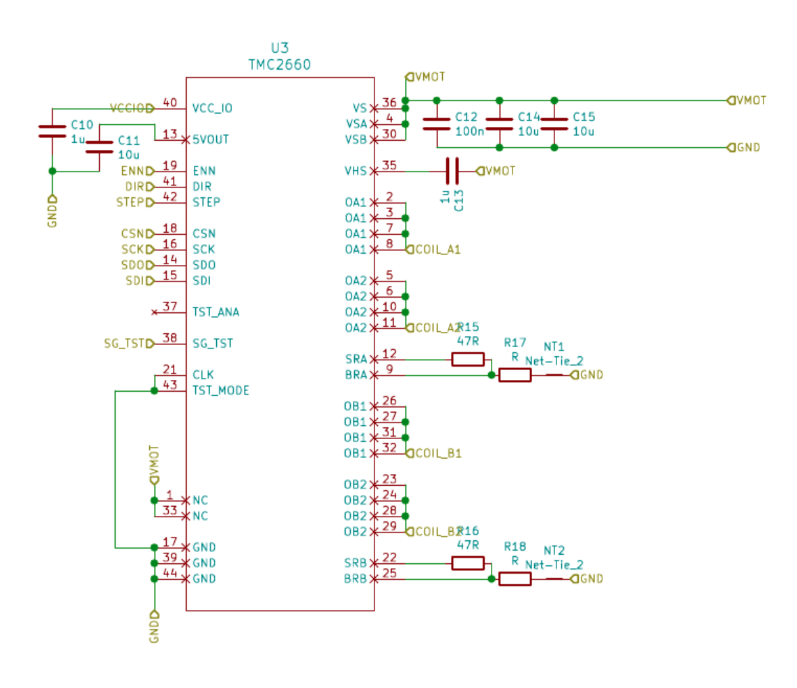
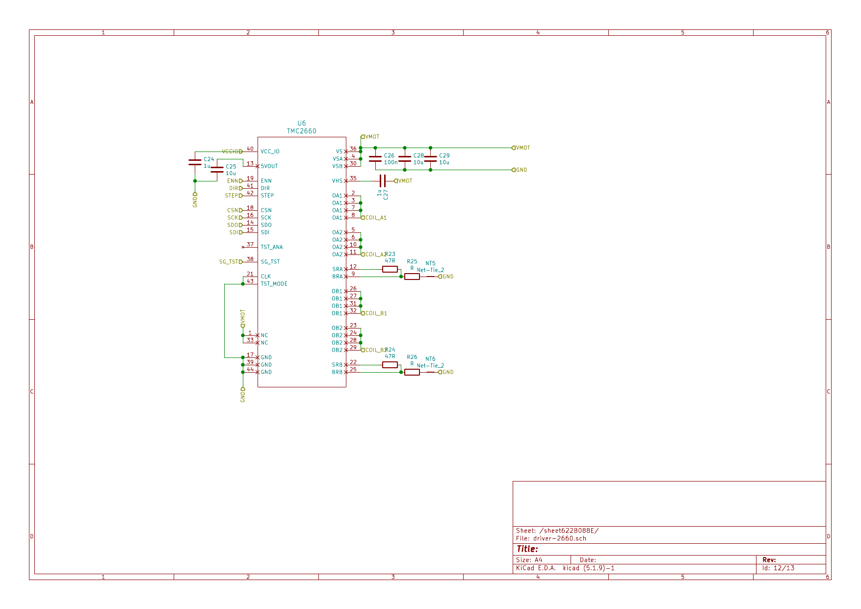
The V2 Prime has 4 onboard TMC2660 stepper drivers. All drivers share an SPI bus and enable signal.
Step and Direction Pins
Driver
Axis
Step Pin
Dir Pin
Chip Select
StallGuard
A
Alpha (X)
PG0
PG1
PJ2
PK0
B
Beta (Y)
PF12
PF11
PB12
PK1
C
Gamma (Z)
PE14
PE15
PJ3
PK2
D
Delta (E)
PE10
PE12
PJ4
PK3
Shared Motor SPI Bus
Function
Smoothie Pin
Description
MOSI
PD14
SPI data to drivers (MOTSPI_COPI)
MISO
PE4
SPI data from drivers (MOTSPI_CIPO)
SCK
PI10
SPI clock (MOTSPI_SCK)
Enable
PH13
Shared enable for all drivers (active low)
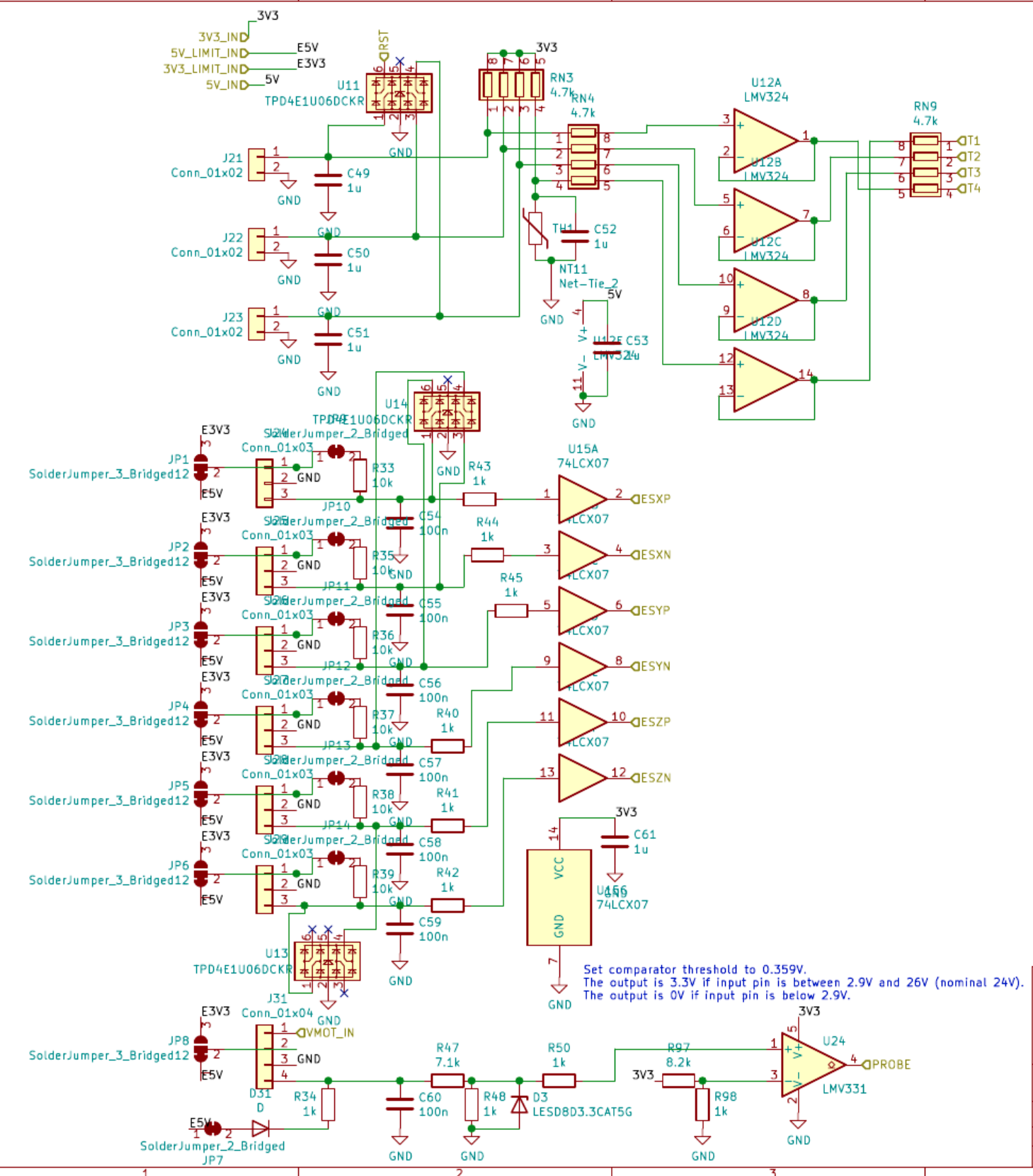
Thermistor/ADC Pins
Thermistor Input Circuit
4 buffered thermistor inputs via LMV324 op-amp
V2 Prime has 4 buffered thermistor inputs via an LMV324 op-amp buffer, plus additional unbuffered ADC channels.
Buffered Thermistor Inputs
Input
Config Pin
STM32 Pin
Connector
Description
T1
ADC1_1
PF11
J25
Thermistor 1 (Hotend)
T2
ADC1_2
PF12
J24
Thermistor 2 (Bed)
T3
ADC1_3
PB0
J26
Thermistor 3
T4
ADC1_0
PA0_C
J27-J29
Board Temperature
Config Format: Use the ADC channel name (e.g., ADC1_1) in your config file, NOT the STM32 pin name. For example: temperature_control.hotend.thermistor_pin = ADC1_1
Voltage Monitoring ADC Channels
Signal
Smoothie Pin
ADC Channel
Divider Ratio
Purpose
VMOT
PC4
ADC1_CH13
11:1
Motor supply voltage
VFET
PC5
ADC1_CH15
11:1
MOSFET supply voltage
Board Temp
TH1
Internal
-
Onboard thermistor
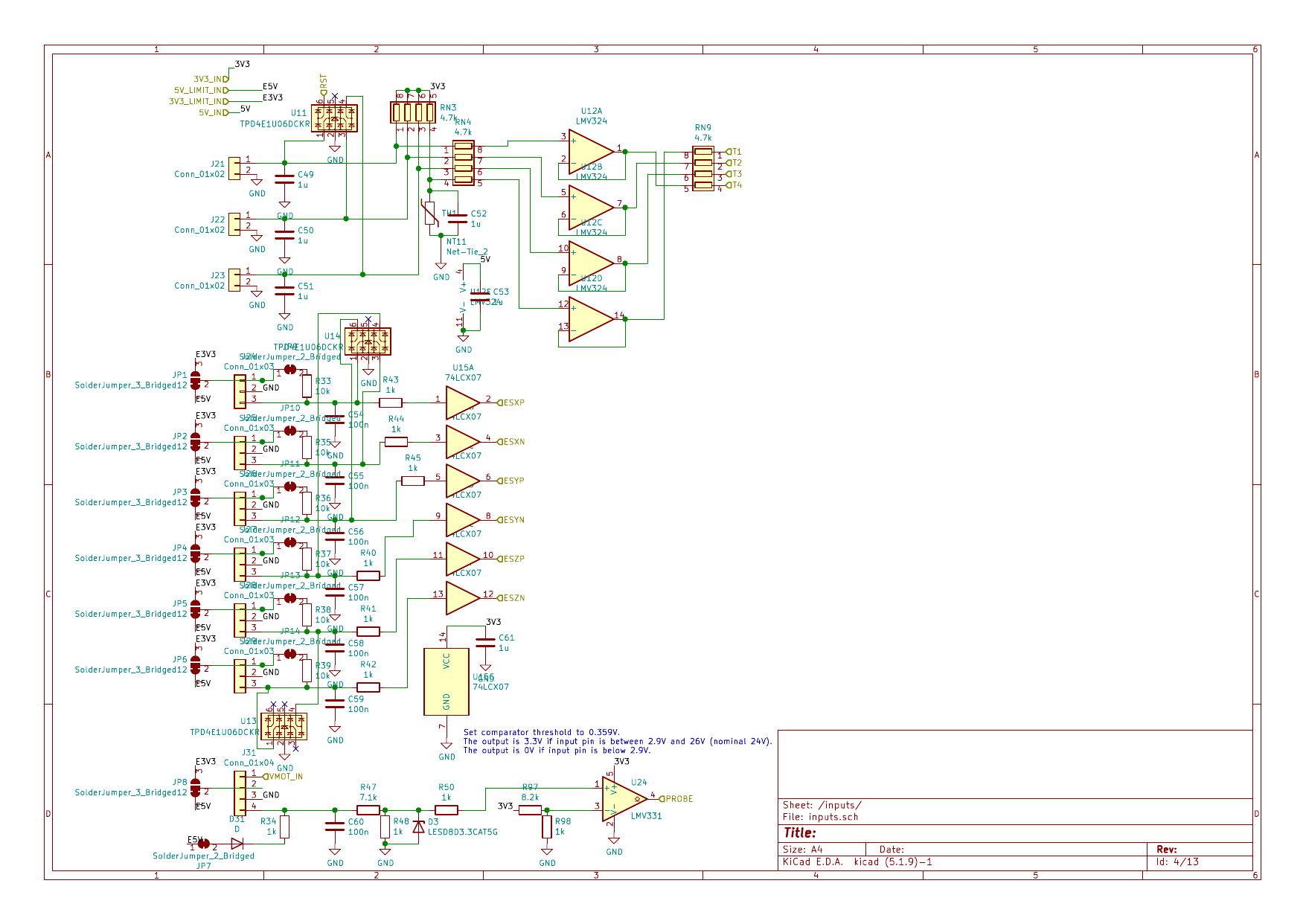
Endstop Pins
Endstop Input Circuit
6 endstops with ESD protection and configurable pull resistors
6 endstop inputs with ESD protection and configurable pull-up/pull-down via solder jumpers.
Endstop
Smoothie Pin
BGA Pin
Signal
Jumper
X Min
PG10
A9
ESXMIN
JP1
X Max
PG9
A10
ESXMAX
JP2
Y Min
PG11
B9
ESYMIN
JP3
Y Max
PG12
C9
ESYMAX
JP4
Z Min
PG13
D9
ESZMIN
JP5
Z Max
PG14
D8
ESZMAX
JP6
Endstop Pull Configuration Jumpers
Each endstop has a 3-way solder jumper (JP1-JP6) to configure pull-up or pull-down:
Position 1-2 (default): Pull to 3.3V
Position 2-3: Pull to GND
Position 2 center: Pull to 5V
Probe Input
Probe Input Circuit
Probe input with comparator and JP7 voltage range selector
Signal
Smoothie Pin
Connector
Description
PROBE
PB0
J22
Probe input via comparator
CRITICAL - JP7 Jumper:
The probe input voltage range is controlled by jumper JP7 (bottom side near probe input):
JP7 intact (default): Input range 0-5V only
JP7 cut: Input range 2.9V to 26V (for 24V inductive probes)
WARNING: Using a >5V probe with JP7 intact will damage the board!
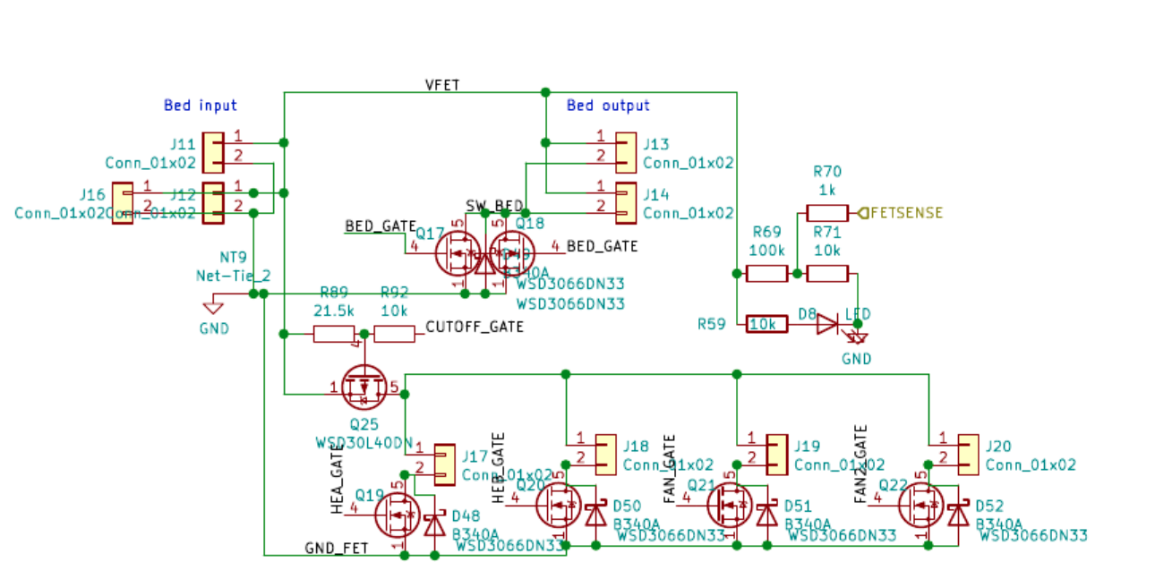
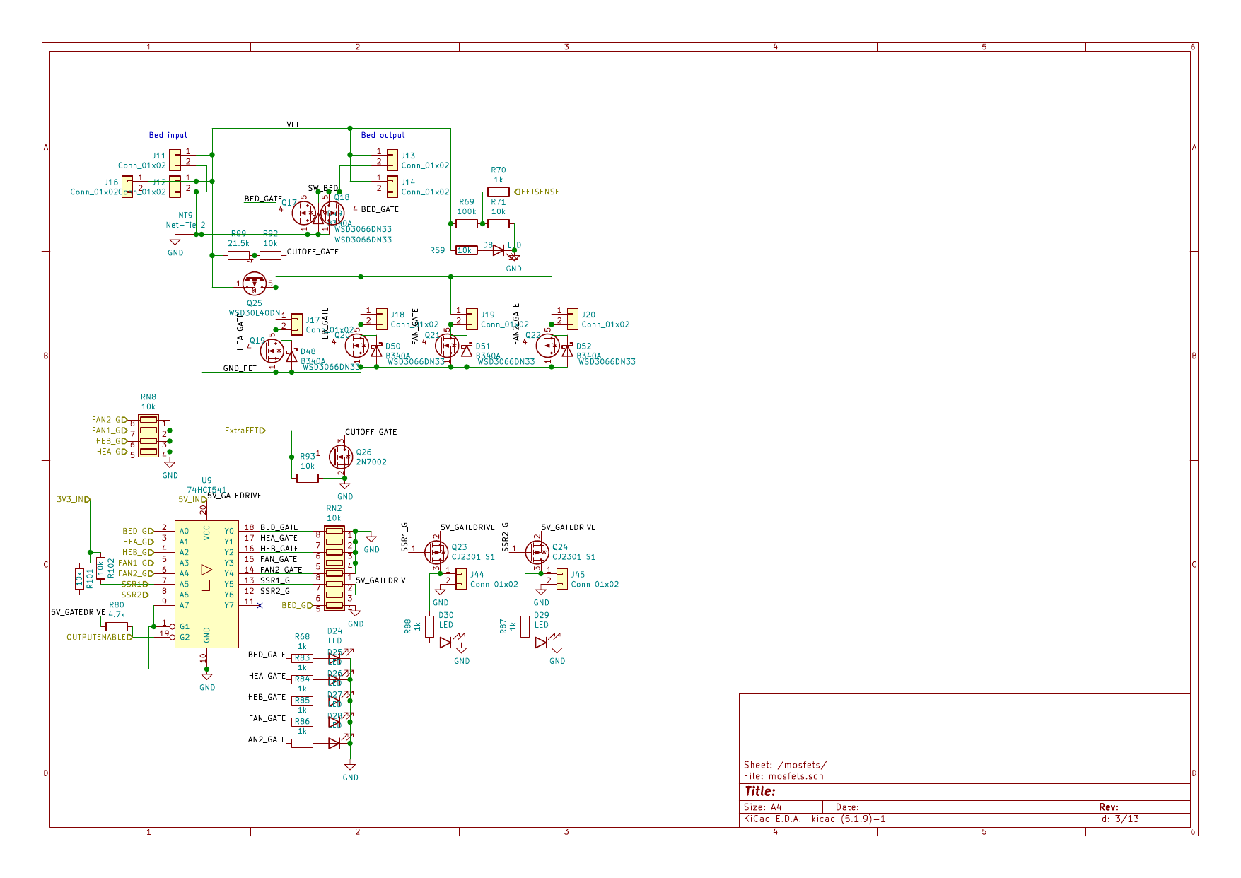
MOSFET Output Pins
MOSFET Output Circuit
Hotend and fan MOSFET outputs with gate driver
Heater and Fan Outputs
Output
Smoothie Pin
Signal
Connector
Current Rating
Hotend A
PJ6
HEA_G
J17
~5A
Hotend B
PJ7
HEB_G
J18
~5A
Fan 1
PJ8
FAN1_G
J19
~5A
Fan 2
PJ9
FAN2_G
J20
~5A
Bed
PJ10
BED_G
J13-J14
~10-12A
Safety Feature: Hotend A, Hotend B, Fan 1, and Fan 2 are controlled by a highside PFET cutoff circuit. The bed FET is independent and not affected by the cutoff.
SSR and Extra Outputs
Output
Smoothie Pin
Signal
Connector
Description
SSR1
PC0
SSR1
J44
Logic-level SSR output
SSR2
PJ11
SSR2
J45
Logic-level SSR output
ExtraFET
PH2
ExtraFET
-
Additional switched output
Output Enable
Signal
Smoothie Pin
Description
OUTPUTENABLE
PJ5
Master enable for all FET outputs
PWM/Timer Pins
V2 has multiple hardware timer channels available for PWM:
Timer 1 Channels
Channel
Smoothie Pin
BGA Pin
Function
TIM1_CH1
PE9
P9
PWM output
TIM1_CH2
PE11
P10
PWM output
TIM1_CH3
PE12
R10
PWM output
TIM1_CH4
PE13
T10
PWM output (spare)
Timer 8 Channels
Channel
Smoothie Pin
BGA Pin
Function
TIM8_CH1
PH6
T11
PWM output
TIM8_CH2
PH8
T13
PWM output
TIM8_CH3
PH9
R13
PWM output
TIM8_CH4
PH7
U13
PWM output
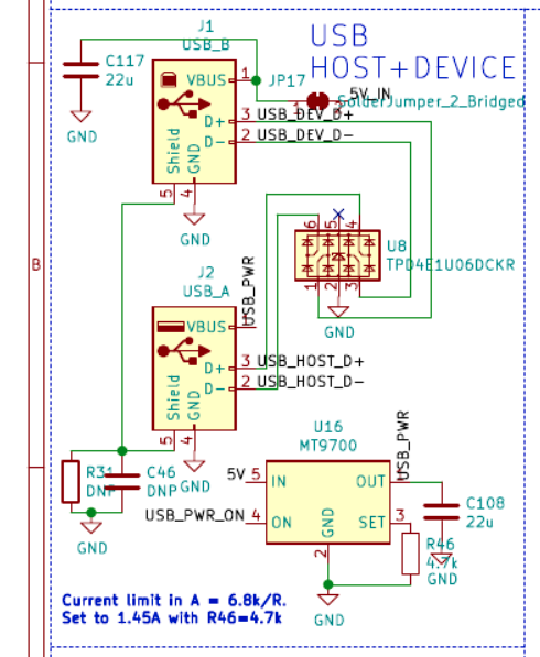
Communication Interfaces
USB Host + Device Circuit
USB-B device connector with SD card interface
USB Device
Signal
Smoothie Pin
BGA Pin
Connector
USB_DEV_D+
PA12
E16
J1 (USB-B)
USB_DEV_D-
PA11
E17
J1 (USB-B)
USB Host
Signal
Smoothie Pin
BGA Pin
Connector
USB_HOST_D+
PB14
U15
J2 (USB-A)
USB_HOST_D-
PB15
T15
J2 (USB-A)
USB_PWR_ON
PB13
U14
Host power control
Note: USB Host functionality has hardware support but firmware is not yet implemented.
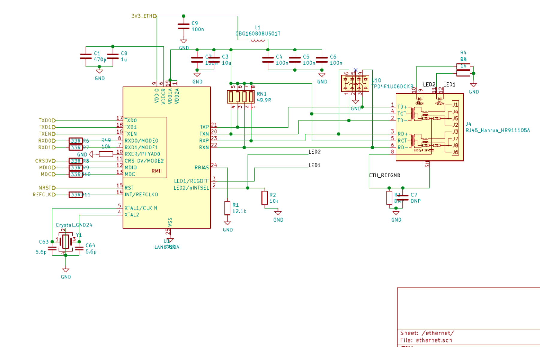
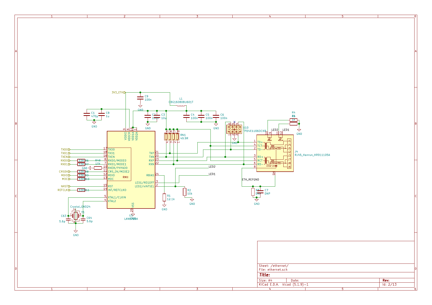
Ethernet (RMII)
Ethernet PHY Circuit
LAN8720A PHY with RJ45 connector and magnetics
Signal
Smoothie Pin
Description
ETH_TXD0
PG13
Transmit data 0
ETH_TXD1
PG12
Transmit data 1
ETH_TXEN
PG11
Transmit enable
ETH_RXD0
PC4
Receive data 0
ETH_RXD1
PC5
Receive data 1
ETH_CRSDV
PA7
Carrier sense/data valid
ETH_MDIO
PA2
Management data I/O
ETH_MDC
PC1
Management data clock
ETH_REFCLK
PA1
50MHz reference clock
I2C Buses
Bus
SDA Pin
SCL Pin
Purpose
I2C2
PB1
PA4
User I2C
I2C3
PH8
PH7
Additional I2C
UART/USART
UART
TX Pin
RX Pin
Purpose
USART3
PD8
PD9
Available on expansion
UART4
PD1
PD0
Available on expansion
SPI Buses
Bus
MOSI
MISO
SCK
Purpose
Motor SPI
PD14
PE4
PI10
TMC2660 drivers
SPI1
PB5
PB4
PB3
User SPI (displays)
Storage
MicroSD (SDIO Interface)
Signal
Smoothie Pin
Description
SD_D0
PC8
Data line 0
SD_D1
PC9
Data line 1
SD_D2
PC10
Data line 2
SD_D3
PC11
Data line 3
SD_CMD
PD2
Command
SD_CK
PC12
Clock
CARD_DET
PG2
Card detection
Performance: V2 uses SDIO interface (10-25 MB/s) instead of V1's SPI interface (~0.5 MB/s) - approximately 20-50× faster!
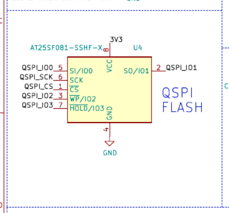
QSPI Flash
QSPI Flash Circuit
Quad-SPI flash for firmware storage
Signal
Smoothie Pin
Description
QSPI_IO0
PD11
Data 0
QSPI_IO1
PD12
Data 1
QSPI_IO2
PE2
Data 2
QSPI_IO3
PD13
Data 3
QSPI_SCK
PB2
Clock
QSPI_CS
PB6
Chip select
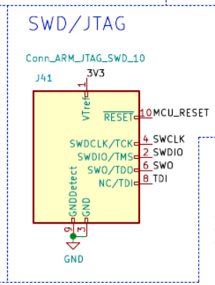
Debug Interface
SWD/JTAG Debug Interface
Standard ARM debug connector with UART
SWD/JTAG (J41)
Pin
Signal
Smoothie Pin
Description
1
VTref
3V3
Reference voltage
2
SWDIO
PA13
Debug data
3
GND
GND
Ground
4
SWCLK
PA14
Debug clock
5
GND
GND
Ground
6
SWO
PB3
Trace output
8
TDI
PA15
JTAG data in
10
RESET
NRST
System reset
Debug UART (J30)
Pin
Signal
Smoothie Pin
Description
1
GND
GND
Ground
2
RX
PD6
MCU receive (connect to TX)
3
TX
PD5
MCU transmit (connect to RX)
Baud rate: 115200 8N1
System Pins
Crystals
Crystal
Frequency
Input Pin
Output Pin
Purpose
HSE
25 MHz
PH0
PH1
Main system clock
LSE
32.768 kHz
PC14
PC15
RTC clock
Boot Configuration
Signal
Smoothie Pin
BGA Pin
Description
BOOT0
BOOT0
E8
Boot mode (LOW=flash, HIGH=DFU)
NRST
NRST
K1
System reset (active low)
Board Detection
Signal
Smoothie Pin
BGA Pin
Description
BDET_PF3
PF3
H4
Board ID bit 0
BDET_PF5
PF5
J4
Board ID bit 1
BDET_PF7
PF7
K3
Board ID bit 2
BDET_PE10
PE10
N9
Board ID bit 3
Board ID values:
ID 0 (0000)
: V2 Prime with TMC2590 drivers
ID 1 (0001)
: V2 Prime with TMC2660 drivers
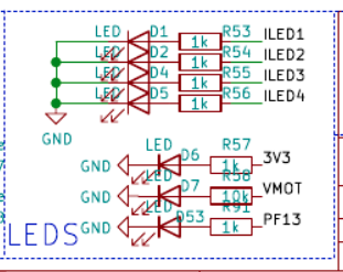
LED Indicators
LED Indicator Circuit
4 debug LEDs showing boot progress
LED
Smoothie Pin
Signal
Description
LED1
PJ14
ILED1
Debug LED 1 (boot phase 4)
LED2
PJ13
ILED2
Debug LED 2 (boot phase 3)
LED3
PJ12
ILED3
Debug LED 3 (boot phase 2)
LED4
PJ15
ILED4
Debug LED 4 (boot phase 1)
MSD
PI0
MSD
Mass storage mode indicator
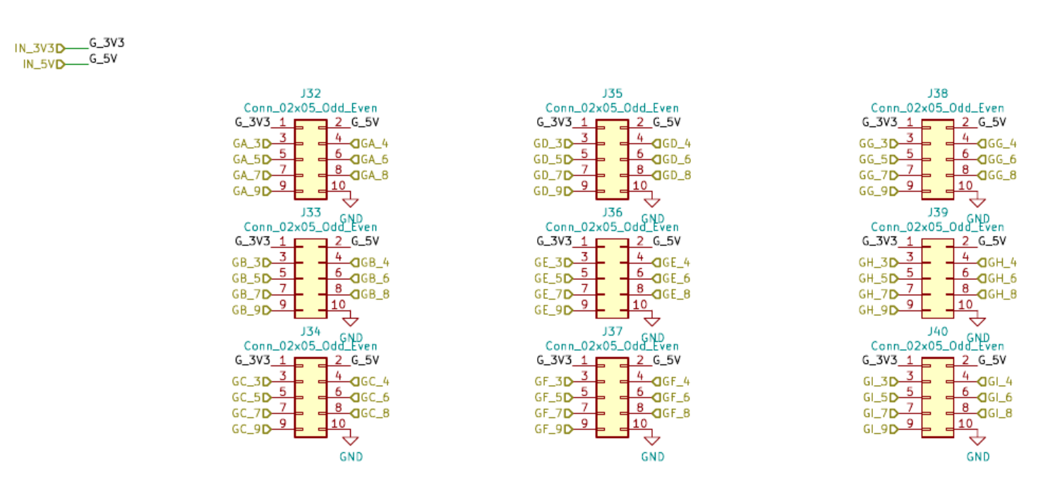
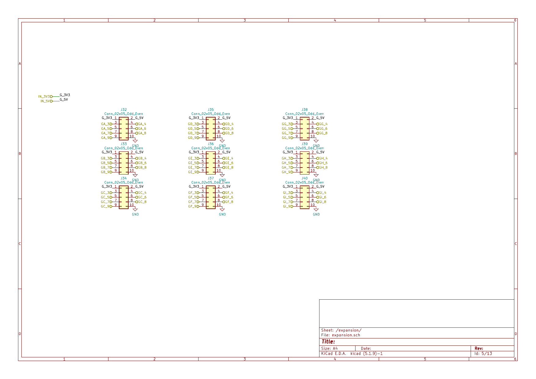
Gadgeteer Expansion Headers
Expansion Headers Schematic
9 Gadgeteer-style 10-pin expansion headers
V2 Prime has 9 Gadgeteer-style 10-pin expansion headers (GA through GI).
Standard Header Pinout
All headers follow this pinout:
Pin
Function
1
3.3V
2
5V
3-9
GPIO (varies by header)
10
GND
Header Pin Assignments
Header GA (J32) - Motor SPI / Encoder
Pin
Smoothie Pin
Alternate Function
3
PJ0
GPIO
4
PJ1
GPIO
5
PI11
GPIO
6
PI12
GPIO
7
PI13
GPIO
8
PI14
GPIO
9
PI15
GPIO
Header GB (J33)
Pin
Smoothie Pin
Alternate Function
3
PK4
GPIO
4
PK5
GPIO
5
PK6
GPIO
6
PK7
GPIO
7
PG3
GPIO
8
PG4
GPIO
9
PG5
GPIO
Header GC (J34)
Pin
Smoothie Pin
Alternate Function
3
PG6
GPIO
4
PG7
GPIO
5
PG8
GPIO
6
PC6
GPIO
7
PC7
GPIO
8
PD15
GPIO
9
PD14
GPIO
Header GD (J35) - UART / PWM
Pin
Smoothie Pin
Alternate Function
3
PD0
UART4_RX
4
PD1
UART4_TX
5
PD3
GPIO
6
PD4
GPIO
7
PD5
USART2_TX
8
PD6
USART2_RX
9
PD7
GPIO
Header GE (J36) - Timer / PWM
Pin
Smoothie Pin
Alternate Function
3
PE0
GPIO
4
PE1
GPIO
5
PE3
GPIO
6
PE5
TIM15_CH1
7
PE6
TIM15_CH2
8
PE7
GPIO
9
PE8
GPIO
Header GF (J37)
Pin
Smoothie Pin
Alternate Function
3
PF0
GPIO
4
PF1
GPIO
5
PF2
GPIO
6
PF4
GPIO
7
PF6
GPIO
8
PF8
GPIO
9
PF9
GPIO
Header GG (J38) - I2C
Pin
Smoothie Pin
Alternate Function
3
PF10
GPIO
4
PF13
GPIO
5
PF14
I2C4_SCL
6
PF15
I2C4_SDA
7
PH3
GPIO
8
PH4
GPIO
9
PH5
GPIO
Header GH (J39) - ADC
Pin
Smoothie Pin
Alternate Function
3
PA3
ADC1_CH15
4
PA5
DAC1_OUT2
5
PA6
ADC1_CH3
6
PB0
ADC1_CH9
7
PB1
ADC1_CH5
8
PA8
GPIO
9
PA9
GPIO
Header GI (J40)
Pin
Smoothie Pin
Alternate Function
3
PA10
GPIO
4
PH10
GPIO
5
PH11
GPIO
6
PH12
GPIO
7
PB10
GPIO
8
PB11
GPIO
9
PH14
GPIO
Complete BGA Pin Reference
ADC Channel Mapping (Thermistors)
The firmware maps ADC channel names to physical pins. Use the Config Pin in your config files:
Config Pin
STM32 Pin
ADC Hardware
Typical Use
ADC1_0
PA0_C
ADC1_INP0
Board Temperature (T4)
ADC1_1
PF11
ADC1_INP2
Thermistor 1 (T1)
ADC1_2
PF12
ADC1_INP6
Thermistor 2 (T2)
ADC1_3
PB0
ADC1_INP9
Thermistor 3 (T3)
ADC1_4
PC2
ADC1_INP12
Expansion (GH)
ADC1_5
PC3
ADC1_INP13
Expansion (GH)
ADC1_6
PA3
ADC1_INP15
Expansion (GH)
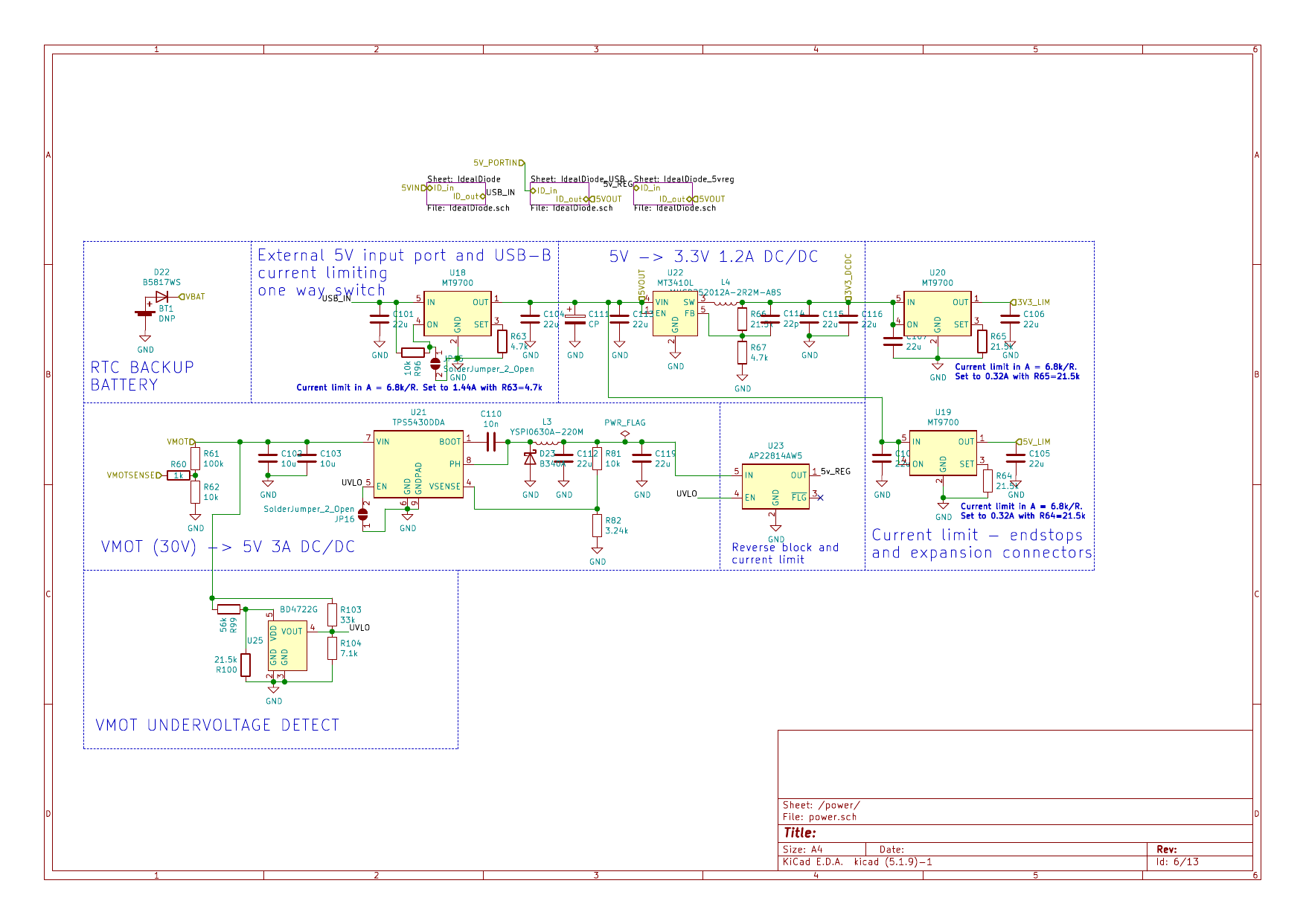
Power Pins Summary
Type
Count
Voltage
VDD
15
3.3V
VSS
30+
GND
VDDA
1
3.3V (analog)
VSSA
1
GND (analog)
VREF+
1
3.3V (ADC ref)
VREF-
1
GND (ADC ref)
VBAT
1
3V (RTC backup)
VDDLDO
3
1.2V (internal)
VCAP
3
1.2V (core caps)
STM32H7 ADC Channels Summary
This table shows the relationship between Smoothieware config names and STM32 hardware.
Config Name
STM32 Pin
ADC Hardware
Assignment
ADC1_0
PA0_C
ADC1_INP0
Board Temperature
ADC1_1
PF11
ADC1_INP2
Thermistor 1
ADC1_2
PF12
ADC1_INP6
Thermistor 2
ADC1_3
PB0
ADC1_INP9
Thermistor 3
ADC1_4
PC2
ADC1_INP12
Expansion (GH)
ADC1_5
PC3
ADC1_INP13
Expansion (GH)
ADC1_6
PA3
ADC1_INP15
Expansion (GH)
ADC3_0
PC0
ADC3_INP10
Voltage Monitor
PC4
PC4
ADC1_INP4
VMOT sense
PC5
PC5
ADC1_INP8
VFET sense
Important: ADC pins are NOT 5V tolerant. Maximum input voltage is 3.3V. The buffered thermistor inputs (T1-T4) have protection circuitry; unbuffered ADC pins on expansion headers do not.
Hardcoded vs Configurable Pins
Hardcoded Pins:
The following pins are hardcoded in firmware and would need source code changes to modify:
USB Device: PA11, PA12
Debug: PA13 (SWDIO), PA14 (SWCLK)
SD Card (SDIO): PC8-PC12, PD2
Crystals: PH0, PH1, PC14, PC15
Motor SPI: PD14, PE4, PI10
Board detect: PF3, PF5, PF7, PE10
All other pins can be reassigned via the configuration file.
Configuration Jumpers Summary
Jumper
Type
Location
Default
Function
JP1-JP6
3-way solder
Near endstops
3.3V pull-up
Endstop pull configuration
JP7
2-way solder
Bottom, near probe
Bridged
Probe voltage range (<5V/2.9-26V)
JP15
2-way solder
Bottom, near 5V
Open
Disable USB 5V input
JP16
2-way solder
Top, near OSHW
Open
Disable onboard 5V regulator
JP17
2-way solder
-
Bridged
Configuration
V1 to V2 Pin Mapping Reference
For users migrating from V1, here’s how key functions map between versions: